
R
12
th
Generation Intel
®
Core
™
Processors
Datasheet, Volume 1 of 2
Rev. 010
February 2023
Doc. No.: 655258, Rev.: 010

You may not use or facilitate the use of this document in connection with any infringement or other legal analysis concerning Intel products described
herein. You agree to grant Intel a non-exclusive, royalty-free license to any patent claim thereafter drafted which includes subject matter disclosed
herein.
No license (express or implied, by estoppel or otherwise) to any intellectual property rights is granted by this document.
All information provided here is subject to change without notice. Contact your Intel representative to obtain the latest Intel product specifications and
roadmaps.
The products described may contain design defects or errors known as errata which may cause the product to deviate from published specifications.
Current characterized errata are available on request.
Intel technologies’ features and benefits depend on system configuration and may require enabled hardware, software or service activation.
Performance varies depending on system configuration. No computer system can be absolutely secure. Check with your system manufacturer or
retailer or learn more at intel.com.
Intel technologies' features and benefits depend on system configuration and may require enabled hardware, software or service activation.
Performance varies depending on system configuration. No computer system can be absolutely secure. Check with your system manufacturer or
retailer or learn more at [intel.com].
*Other names and brands may be claimed as the property of others.
Copyright
©
2021–2022, Intel Corporation. All rights reserved.
R
12
th
Generation Intel
®
Core
™
Processors
Datasheet, Volume 1 of 2 February 2023
2 Doc. No.: 655258, Rev.: 010

Contents
Revision History................................................................................................................11
1.0 Introduction................................................................................................................13
1.1 Processor Volatility Statement................................................................................ 18
1.2 Package Support...................................................................................................18
1.3 Supported Technologies......................................................................................... 19
1.3.1 API Support (Windows*)............................................................................20
1.4 Power Management Support...................................................................................21
1.4.1 Processor Core Power Management............................................................. 21
1.4.2 System Power Management........................................................................21
1.4.3 Memory Controller Power Management........................................................ 21
1.4.4 Processor Graphics Power Management........................................................21
1.5 Thermal Management Support................................................................................22
1.6 Ball-out Information..............................................................................................22
1.7 Processor Testability..............................................................................................22
1.8 Operating Systems Support....................................................................................23
1.9 Terminology and Special Marks............................................................................... 23
1.10 Related Documents............................................................................................. 26
2.0 Technologies...............................................................................................................27
2.1 Platform Environmental Control Interface................................................................. 27
2.1.1 PECI Bus Architecture................................................................................27
2.2 Intel
®
Virtualization Technology.............................................................................. 29
2.2.1 Intel
®
VT for Intel
®
64 and Intel
®
Architecture ..............................................30
2.2.2 Intel
®
Virtualization Technology for Directed I/O........................................... 32
2.2.3 Intel
®
APIC Virtualization Technology (Intel
®
APICv)..................................... 35
2.2.4 Hypervisor-Managed Linear Address Translation............................................ 35
2.3 Security Technologies............................................................................................ 36
2.3.1 Intel
®
Trusted Execution Technology............................................................36
2.3.2 Intel
®
Advanced Encryption Standard New Instructions .................................37
2.3.3 Perform Carry-Less Multiplication Quad Word Instruction ............................... 38
2.3.4 Intel
®
Secure Key..................................................................................... 38
2.3.5 Execute Disable Bit .................................................................................. 38
2.3.6 Boot Guard Technology ............................................................................. 38
2.3.7 Intel
®
Supervisor Mode Execution Protection................................................ 39
2.3.8 Intel
®
Supervisor Mode Access Protection.................................................... 39
2.3.9 Intel
®
Secure Hash Algorithm Extensions.................................................... 39
2.3.10 User Mode Instruction Prevention.............................................................. 40
2.3.11 Read Processor ID................................................................................... 40
2.3.12 Intel
®
Total Memory Encryption - Multi-Key................................................ 40
2.3.13 Intel
®
Control-flow Enforcement Technology............................................... 41
2.3.14 KeyLocker Technology..............................................................................42
2.3.15 Devil’s Gate Rock.................................................................................... 42
2.4 Power and Performance Technologies.......................................................................42
2.4.1 Intel
®
Smart Cache Technology.................................................................. 42
2.4.2 IA Cores Level 1 and Level 2 Caches ...........................................................43
2.4.3 Ring Interconnect..................................................................................... 43
2.4.4 Intel
®
Performance Hybrid Architecture ....................................................... 44
R
Contents—12th Generation Intel
®
Core
™
Processors
12
th
Generation Intel
®
Core
™
Processors
February 2023 Datasheet, Volume 1 of 2
Doc. No.: 655258, Rev.: 010 3

2.4.5 Intel
®
Turbo Boost Max Technology 3.0........................................................44
2.4.6 Intel
®
Hyper-Threading Technology............................................................. 44
2.4.7 Intel
®
Turbo Boost Technology 2.0.............................................................. 45
2.4.8 Enhanced Intel SpeedStep
®
Technology....................................................... 46
2.4.9 Intel
®
Thermal Velocity Boost (Intel
®
TVB)....................................................46
2.4.10 Intel
®
Speed Shift Technology ..................................................................47
2.4.11 Intel
®
Advanced Vector Extensions 2 (Intel
®
AVX2) .................................... 47
2.4.12 Intel
®
64 Architecture x2APIC...................................................................47
2.4.13 Intel
®
Dynamic Tuning Technology............................................................ 49
2.4.14 Intel
®
GMM and Neural Network Accelerator................................................49
2.4.15 Cache Line Write Back............................................................................. 50
2.4.16 Remote Action Request............................................................................ 51
2.4.17 User Mode Wait Instructions .................................................................... 51
2.5 Intel
®
Image Processing Unit.................................................................................. 52
2.5.1 Platform Imaging Infrastructure..................................................................52
2.5.2 Intel
®
Image Processing Unit...................................................................... 52
2.6 Debug Technologies ............................................................................................. 53
2.6.1 Intel
®
Processor Trace .............................................................................. 53
2.6.2 Platform CrashLog.....................................................................................53
2.6.3 Telemetry Aggregator................................................................................ 53
2.7 Clock Topology..................................................................................................... 54
2.7.1 Integrated Reference Clock PLL...................................................................55
2.8 Intel Volume Management Device Technology .......................................................... 55
2.9 Deprecated Technologies........................................................................................57
3.0 Power Management.................................................................................................... 58
3.1 Advanced Configuration and Power Interface (ACPI) States Supported......................... 59
3.2 Processor IA Core Power Management..................................................................... 60
3.2.1 OS/HW Controlled P-states.........................................................................61
3.2.2 Low-Power Idle States............................................................................... 61
3.2.3 Requesting the Low-Power Idle States......................................................... 62
3.2.4 Processor IA Core C-State Rules..................................................................62
3.2.5 Package C-States......................................................................................63
3.2.6 Package C-States and Display Resolutions.................................................... 66
3.3 Processor AUX Power Management ........................................................................66
3.4 Processor Graphics Power Management ...................................................................67
3.4.1 Memory Power Savings Technologies........................................................... 67
3.4.2 Display Power Savings Technologies............................................................ 67
3.4.3 Processor Graphics Core Power Savings Technologies.....................................68
3.5 System Agent Enhanced Intel SpeedStep
®
Technology...............................................69
3.6 Rest Of Platform (ROP) PMIC ................................................................................. 69
3.7 PCI Express* Power Management............................................................................70
3.8 TCSS Power State................................................................................................ 70
4.0 Thermal Management................................................................................................. 72
4.1 Processor Thermal Management..............................................................................72
4.1.1 Thermal Considerations............................................................................. 72
4.1.2 Assured Power (cTDP) .............................................................................. 75
4.1.3 Thermal Management Features................................................................... 76
4.1.4 Intel
®
Memory Thermal Management ......................................................... 83
4.2 Processor Line Thermal and Power Specifications...................................................... 83
R
12th Generation Intel
®
Core
™
Processors—Contents
12
th
Generation Intel
®
Core
™
Processors
Datasheet, Volume 1 of 2 February 2023
4 Doc. No.: 655258, Rev.: 010

4.2.1 Processor Line Power and Frequency Specifications........................................85
4.2.2 Processor Line Thermal and Power.............................................................. 89
4.3 Thermal Profile for PCG 2020 Processor................................................................... 97
4.3.1 Thermal Profile for PCG 2022E Processor......................................................97
4.3.2 Thermal Profile for PCG 2020A Processor......................................................99
4.3.3 Thermal Profile for PCG 2020C Processor....................................................100
4.3.4 Thermal Profile for PCG 2020D Processor....................................................102
4.4 Thermal Metrology ............................................................................................. 102
4.5 Fan Speed Control Scheme with DTS..................................................................... 103
5.0 Memory.....................................................................................................................107
5.1 System Memory Interface.................................................................................... 107
5.1.1 Processor SKU Support Matrix...................................................................107
5.1.2 Supported Memory Modules and Devices.................................................... 109
5.1.3 System Memory Timing Support................................................................113
5.1.4 Memory Controller (MC)...........................................................................115
5.1.5 Memory Controller Power Gate..................................................................115
5.1.6 System Memory Controller Organization Mode (DDR4/5 Only)....................... 115
5.1.7 System Memory Frequency.......................................................................117
5.1.8 Technology Enhancements of Intel
®
Fast Memory Access (Intel
®
FMA)............ 117
5.1.9 Data Scrambling..................................................................................... 118
5.1.10 Data Swapping .....................................................................................118
5.1.11 LPDDR5/x Ascending and Descending......................................................118
5.1.12 LPDDR4x CMD Mirroring ........................................................................ 119
5.1.13 DDR I/O Interleaving............................................................................. 119
5.1.14 DRAM Clock Generation .........................................................................120
5.1.15 DRAM Reference Voltage Generation ....................................................... 120
5.1.16 Data Swizzling...................................................................................... 121
5.1.17 Error Correction With Standard RAM........................................................ 121
5.1.18 Post Package Repair (PPR)..................................................................... 121
5.2 Integrated Memory Controller (IMC) Power Management.......................................... 121
5.2.1 Disabling Unused System Memory Outputs................................................. 121
5.2.2 DRAM Power Management and Initialization................................................ 121
5.2.3 DDR Electrical Power Gating..................................................................... 124
5.2.4 Power Training........................................................................................ 124
6.0 USB-C* Sub System.................................................................................................. 125
6.1 General Capabilities.............................................................................................125
6.2 USB
™
4 Router....................................................................................................127
6.2.1 USB 4 Host Router Implementation Capabilities...........................................127
6.3 USB-C Sub-system xHCI/xDCI Controllers ............................................................. 128
6.3.1 USB 3 Controllers....................................................................................128
6.3.2 USB-C Sub-System PCIe Interface.............................................................129
6.4 USB-C Sub-System Display Interface..................................................................... 129
7.0 PCIe* Interface........................................................................................................ 130
7.1 Processor PCI Express* Interface.......................................................................... 130
7.1.1 PCI Express* Support.............................................................................. 130
7.1.2 PCI Express* Architecture........................................................................ 133
7.1.3 PCI Express* Configuration Mechanism ..................................................... 134
7.1.4 PCI Express* Equalization Methodology .....................................................134
7.1.5 PCI Express* Hot Plug............................................................................ 135
R
Contents—12th Generation Intel
®
Core
™
Processors
12
th
Generation Intel
®
Core
™
Processors
February 2023 Datasheet, Volume 1 of 2
Doc. No.: 655258, Rev.: 010 5

8.0 Direct Media Interface and On Package Interface..................................................... 136
8.1 Direct Media Interface (DMI)................................................................................ 136
8.1.1 DMI Lane Reversal and Polarity Inversion................................................... 136
8.1.2 DMI Error Flow........................................................................................137
8.1.3 DMI Link Down....................................................................................... 137
8.2 On Package Interface (OPI).................................................................................. 137
8.2.1 OPI Support........................................................................................... 138
8.2.2 Functional Description..............................................................................138
9.0 Graphics....................................................................................................................139
9.1 Processor Graphics..............................................................................................139
9.1.1 Media Support (Intel
®
QuickSync and Clear Video Technology HD)................. 139
9.2 Platform Graphics Hardware Feature .....................................................................142
9.2.1 Hybrid Graphics...................................................................................... 142
10.0 Display.................................................................................................................... 143
10.1 Display Technologies Support..............................................................................143
10.2 Display Configuration.........................................................................................143
10.3 Display Features................................................................................................146
10.3.1 General Capabilities............................................................................... 146
10.3.2 Multiple Display Configurations................................................................147
10.3.3 High-bandwidth Digital Content Protection (HDCP)..................................... 147
10.3.4 DisplayPort*......................................................................................... 147
10.3.5 High-Definition Multimedia Interface (HDMI*)........................................... 150
10.3.6 embedded DisplayPort* (eDP*)............................................................... 151
10.3.7 MIPI* DSI............................................................................................ 152
10.3.8 Integrated Audio................................................................................... 153
11.0 Camera/MIPI.......................................................................................................... 155
11.1 Camera Pipe Support......................................................................................... 155
11.2 MIPI* CSI-2 Camera Interconnect....................................................................... 155
11.2.1 Camera Control Logic.............................................................................156
11.2.2 Camera Modules....................................................................................156
11.2.3 CSI-2 Lane Configuration........................................................................156
12.0 Signal Description................................................................................................... 157
12.1 System Memory Interface...................................................................................158
12.1.1 DDR4 Memory Interface......................................................................... 158
12.1.2 LP4x-LP5 Memory Interface .................................................................. 160
12.1.3 DDR5 Memory Interface......................................................................... 162
12.2 PCI Express* Graphics (PEG) Signals................................................................... 164
12.3 Direct Media Interface (DMI) Signals....................................................................164
12.4 Reset and Miscellaneous Signals.......................................................................... 165
12.5 Display Interfaces .............................................................................................167
12.5.1 Digital Display Interface (DDI) Signals..................................................... 167
12.5.2 Digital Display Audio Signals................................................................... 167
12.6 USB Type-C Signals........................................................................................... 167
12.7 MIPI* CSI-2 Interface Signals............................................................................ 168
12.8 Processor Clocking Signals..................................................................................169
12.9 Testability Signals..............................................................................................169
12.10 Error and Thermal Protection Signals..................................................................170
R
12th Generation Intel
®
Core
™
Processors—Contents
12
th
Generation Intel
®
Core
™
Processors
Datasheet, Volume 1 of 2 February 2023
6 Doc. No.: 655258, Rev.: 010

12.11 Power Sequencing Signals................................................................................ 171
12.12 Processor Power Rails.......................................................................................172
12.13 Ground and Reserved Signals............................................................................173
12.14 Processor Internal Pull-Up / Pull-Down Terminations.............................................174
13.0 Electrical Specifications.......................................................................................... 175
13.1 Processor Power Rails........................................................................................ 175
13.1.1 Power and Ground Pins.......................................................................... 175
13.1.2 Voltage Regulator.................................................................................. 175
13.1.3 V
CC
Voltage Identification (VID)...............................................................176
13.2 DC Specifications.............................................................................................. 176
13.2.1 Processor Power Rails DC Specifications....................................................176
13.2.2 Processor Interfaces DC Specifications..................................................... 191
14.0 Package Mechanical Specifications......................................................................... 201
14.1 Package Mechanical Attributes............................................................................ 201
14.2 Package Storage Specifications........................................................................... 203
15.0 CPU And Device IDs................................................................................................ 205
15.1 CPUID..............................................................................................................205
15.2 PCI Configuration Header................................................................................... 206
15.3 Device IDs........................................................................................................206
R
Contents—12th Generation Intel
®
Core
™
Processors
12
th
Generation Intel
®
Core
™
Processors
February 2023 Datasheet, Volume 1 of 2
Doc. No.: 655258, Rev.: 010 7

Figures
1 S Processor Line Platform Diagram.............................................................................15
2 H/P Processor Line Platform Diagram..........................................................................15
3 U15 Processor Line Platform Diagram......................................................................... 16
4 U9 Processor Line Platform Diagram...........................................................................17
5 HX Processor Line Platform Diagram...........................................................................18
6 Example for PECI Host-Clients Connection...................................................................28
7 Example for PECI EC Connection................................................................................29
8 Device to Domain Mapping Structures ....................................................................... 33
9 Hybrid Cache.......................................................................................................... 43
10 Processor Camera System........................................................................................ 52
11 Telemetry Aggregator...............................................................................................54
12 Processor Power States............................................................................................ 58
13 Processor Package and IA Core C-States.....................................................................59
14 Idle Power Management Breakdown of the Processor IA Cores.......................................61
15 Package C-State Entry and Exit................................................................................. 64
16 Package Power Control............................................................................................. 74
17 PROCHOT Demotion Signal Description ......................................................................81
18 Thermal Profile for PCG 2022E Processor ................................................................... 97
19 Thermal Profile for PCG 2020A Processor ................................................................... 99
20 Thermal Profile for PCG 2020C Processor ................................................................. 100
21 Thermal Test Vehicle Thermal Profile for PCG 2020D Processor ....................................102
22 Thermal Test Vehicle (TTV) Case Temperature (T
CASE
) Measurement Location ................103
23 Digital Thermal Sensor (DTS) 1.1 Definition Points .................................................... 104
24 Digital Thermal Sensor (DTS) 2.0 Definition Points..................................................... 106
25 Intel
®
DDR4/5 Flex Memory Technology Operations.................................................... 116
26 DDR4 Interleave (IL) and Non-Interleave (NIL) Modes Mapping....................................120
27 PCI Express* Related Register Structures in the Processor ..........................................134
28 Example for DMI Lane Reversal Connection............................................................... 137
29 S Processor Display Architecture.............................................................................. 145
30 H/P/U Processor Display Architecture........................................................................146
31 DisplayPort* Overview............................................................................................148
32 HDMI* Overview ...................................................................................................151
33 MIPI* DSI Overview...............................................................................................153
34 Input Device Hysteresis ......................................................................................... 200
R
12th Generation Intel
®
Core
™
Processors—Figures
12
th
Generation Intel
®
Core
™
Processors
Datasheet, Volume 1 of 2 February 2023
8 Doc. No.: 655258, Rev.: 010

Tables
1 Processor Lines ...................................................................................................... 13
2 Terminology............................................................................................................23
3 Special Marks .........................................................................................................26
4 System States ........................................................................................................59
5 Integrated Memory Controller (IMC) States ................................................................60
6 G, S, and C Interface State Combinations .................................................................. 60
7 Core C-states .........................................................................................................63
8 Package C-States.................................................................................................... 64
9 Package C-States with PCIe* Link States Dependencies ............................................... 70
10 TCSS Power State ...................................................................................................70
11 Assured Power Modes...............................................................................................76
12 Processor Base Power (TDP) and Frequency Specifications(H-Processor Line, P-
Processor Line) ...................................................................................................... 85
13 Processor Base Power (TDP) and Frequency Specifications(U-Processor Line) ..................86
14 Processor Base Power (TDP) and Frequency Specifications (U 9W-Processor Line) ........... 87
15 Processor Base Power (TDP) and Frequency Specifications (S-Processor Line) ................. 87
16 Processor Base Power (TDP) and Frequency Specifications (HX-Processor Line) ............... 89
17 Package Turbo Specifications (H/P/U -Processor Lines) .................................................89
18 Junction Temperature Specifications (H / HX /P/U - Processor Lines) ..............................92
19 Package Turbo Specifications (S / HX - Processor Lines) ...............................................92
20 Low Power and TTV Specifications (S-Processor Line LGA )............................................95
21 TCONTROL Offset Configuration (S-Processor Line - Client) ......................................... 96
22 Thermal Test Vehicle Thermal Profile for PCG 2022E Processor....................................... 97
23 Thermal Test Vehicle Thermal Profile for PCG 2020A Processor.......................................99
24 Thermal Test Vehicle Thermal Profile for PCG 2020C Processor..................................... 101
25 Thermal Test Vehicle Thermal Profile for PCG 2020D Processor ....................................102
26 Digital Thermal Sensor (DTS) 1.1 Thermal Solution Performance Above T
CONTROL
............105
27 Thermal Margin Slope.............................................................................................106
28 DDR Support Matrix Table....................................................................................... 107
29 DDR Technology Support Matrix...............................................................................108
30 Supported DDR4 Non-ECC SoDIMM Module Configurations (S/H/P/U15-Processor Line)...109
31 Supported DDR4 ECC SoDIMM Module Configurations (S-Processor Line) ......................109
32 Supported DDR4 Non-ECC UDIMM Module Configurations (S-Processor Line) ................ 109
33 Supported DDR4 ECC UDIMM Module Configurations (S-Processor Line) ....................... 110
34 Supported DDR5 Non-ECC SoDIMM Module Configurations (S/H/P/U15-Processor Line)...110
35 Supported DDR5 ECC SoDIMM Module Configurations (S-Processor Line) ......................110
36 Supported DDR5 Non-ECC UDIMM Module Configurations (S-Processor Line) ................ 110
37 Supported DDR5 ECC UDIMM Module Configurations (S-Processor Line)........................ 110
38 Supported DDR4 Memory Down Device Configurations (H/P /U15 Processor Line) ..........111
39 Supported DDR5 Memory Down Device Configurations (H/P/U15 Processor Line) ...........111
40 Supported LPDDR4x x32 DRAMs Configurations (H/P/U Processor Line) .......................111
41 Supported LPDDR4x x64 DRAMs Configurations (H/P/U Processor Line) .......................112
42 Supported LPDDR5/x x32 DRAMs Configurations
6
(H/P/U Processor Line) .................... 112
43 Supported LPDDR5/x x64 DRAMs Configurations
4
(H/P/U Processor Line) .................... 112
44 DDR System Memory Timing Support....................................................................... 113
45 LPDDR System Memory Timing Support ................................................................... 113
46 SA Speed Enhanced Speed Steps (SA-GV) and Gear Mode Frequencies ........................ 114
47 Interleave (IL) and Non-Interleave (NIL) Modes Pin Mapping ...................................... 119
48 USB-C* Port Configuration...................................................................................... 126
49 USB-C* Lanes Configuration....................................................................................126
50 USB-C* Non-Supported Lane Configuration............................................................... 127
51 PCIe via USB4 Configuration................................................................................... 129
52 PCI Express* 16 - Lane Bifurcation and Lane Reversal Mapping....................................131
53 S- Processor PCI Express* 4 - Lane Reversal Mapping ................................................132
R
Tables—12th Generation Intel
®
Core
™
Processors
12
th
Generation Intel
®
Core
™
Processors
February 2023 Datasheet, Volume 1 of 2
Doc. No.: 655258, Rev.: 010 9

54 H-Processor Line PCI Express* 8 - Lane Reversal Mapping...........................................132
55 H/P/U15-Processor Line PCI Express* 4 - Lane Reversal Mapping ................................ 132
56 U9-Processor PCI Express* 4 - Lane Reversal Mapping ...............................................133
57 PCI Express* Maximum Transfer Rates and Theoretical Bandwidth ...............................133
58 Hardware Accelerated Video Decoding ..................................................................... 140
59 Hardware Accelerated Video Encode ........................................................................ 141
60 Display Ports Availability and Link Rate for H/P/U - Processor Lines ..............................143
61 Display Resolutions and Link Bandwidth for Multi-Stream Transport Calculations.............149
62 DisplayPort Maximum Resolution..............................................................................149
63 HDMI Maximum Resolution..................................................................................... 151
64 Embedded DisplayPort Maximum Resolution.............................................................. 152
65 MIPI* DSI Maximum Resolution .............................................................................. 153
66 Processor Supported Audio Formats over HDMI* and DisplayPort*................................153
67 CSI-2 Lane Configuration for H/P/U-Processor Lines................................................... 156
68 Signal Tables Terminology ...................................................................................... 157
69 DDR4 Memory Interface......................................................................................... 158
70 DDR5 Memory Interface......................................................................................... 162
71 Error and Thermal Protection Signals........................................................................170
72 Power Sequencing Signals ......................................................................................171
73 Processor Power Rails Signals ................................................................................. 172
74 Processor Ground Rails Signals ............................................................................... 173
75 GND, RSVD, and NCTF Signals.................................................................................174
76 Processor VCC
CORE
Active and Idle Mode DC Voltage and Current Specifications .............176
77 VccIN_AUX Supply DC Voltage and Current Specifications........................................... 181
78 Processor Graphics (VccGT) Supply DC Voltage and Current Specifications.....................184
79 Processor Graphics (VccSA) Supply DC Voltage and Current Specifications.....................186
80 Memory Controller (VDD2) Supply DC Voltage and Current Specifications .................... 187
81 VCCANA Supply DC Voltage and Current Specifications ............................................. 188
82 VCC_MIPILP Supply DC Voltage and Current Specifications ........................................ 188
83 Vcc
1P05_PROC
Supply DC Voltage and Current Specifications..........................................188
84 Vcc
1P8_PROC
Supply DC Voltage and Current Specifications .......................................... 189
85 DDR4 Signal Group DC Specifications ...................................................................... 191
86 DDR5 Signal Group DC Specifications....................................................................... 192
87 LPDDR4x Signal Group DC Specifications ................................................................. 193
88 LPDDR5 Signal Group DC Specifications ................................................................... 195
89 PCI Express* Graphics (PEG) Group DC Specifications................................................ 196
90 DSI HS Transmitter DC Specifications....................................................................... 197
91 DSI LP Transmitter DC Specifications........................................................................ 197
92 Display Audio and Utility Pins DC Specification........................................................... 198
93 CMOS Signal Group DC Specifications ......................................................................198
94 GTL Signal Group and Open Drain Signal Group DC Specifications................................ 198
95 PECI DC Electrical Limits.........................................................................................199
96 S LGA Processor Package Mechanical Attributes......................................................... 201
97 HX BGA Processor Package Mechanical Attributes....................................................... 202
98 H/P/U15 - Processor Package Mechanical Attributes....................................................202
99 U9 - Processor Package Mechanical Attributes............................................................203
100 CPUID Format....................................................................................................... 205
101 PCI Configuration Header........................................................................................206
102 Host Device ID (DID0)............................................................................................206
103 Processor Graphics Device ID (DID2)........................................................................207
104 Other Device ID.....................................................................................................208
R
12th Generation Intel
®
Core
™
Processors—Tables
12
th
Generation Intel
®
Core
™
Processors
Datasheet, Volume 1 of 2 February 2023
10 Doc. No.: 655258, Rev.: 010

Revision History
Document
Number
Revision
Number
Description Revision
Date
655258 001 Initial Release for S 125W SKUs October
2021
655258 002 Intel
®
Hybrid Technology name replaced with Intel's Performance Hybrid
Architecture
November
2021
655258 003 Graphics on page 139
• Added the Direct3D12 Video API support and E2E playback information into
the Note in Hardware Accelerated Video Decode on page 139
• Updated the
— Table 58 on page 140
— Intel
®
Media SDK to OneVPL
— Intel
®
CUI SDK to Intel
®
Graphics Control Library
• Removed
— Note of HEVC -10 bit support in Hardware Accelerated Video Decode on
page 139
— Image stabilization in Hardware Accelerated Video Processing on page 141
Signal Description on page 157
• Updated rail for BPM#[3:0] in Processor Internal Pull-Up / Pull-Down
Terminations on page 174
Memory on page 107
• Added
— ECC note in Table 28 on page 107
— Note for S 125W processors in SAGV Points on page 113
Thermal Management on page 72
• Updated DT new SKUs options
December
2021
655258 004 Initial Release for H45 and S 35W, 46W, 58W, 60W, and 65W SKUs
• Added
— Note in Intel
®
Multi-Key Total Memory Encryption
January
2022
655258 005 Initial Release for U9, U15, and P SKUs March 2022
655258 006 Technologies on page 27
• Updated Intel
®
Performance Hybrid Architecture on page 44
Thermal Management on page 72
• Added
— 150W SKU information in Processor Line Power and Frequency Specifications
on page 85 and Processor Line Thermal and Power on page 89
— Thermal Profile for PCG 2022E Processor on page 97
• Updated Fan Speed Control Scheme with DTS on page 103
Memory on page 107
• Updated Processor SKU Support Matrix on page 107
Electrical Specifications on page 175
• Updated CMOS DC Specifications on page 198
April 2022
655258 007 Initial Release for HX SKUs
Introduction on page 13
• Updated API Support (Windows*) on page 20
Memory on page 107
May 2022
continued...
R
Revision History—12th Generation Intel
®
Core
™
Processors
12
th
Generation Intel
®
Core
™
Processors
February 2023 Datasheet, Volume 1 of 2
Doc. No.: 655258, Rev.: 010 11
Document
Number
Revision
Number
Description Revision
Date
• Updated SAGV Points on page 113
Electrical Specifications on page 175
• Updated Vcc
1P05_PROC
DC Specifications on page 188
655258 008 Technologies on page 27
• Corrected L1 Data and Instruction Cache size in IA Cores Level 1 and Level 2
Caches on page 43
Electrical Specifications on page 175
• Added S 6+0 -Processor detail in VCCCORE Iccmax in DC Specifications on page
176
June 2022
655258 009 Technologies on page 27
• Updated Intel
®
Total Memory Encryption - Multi-Key on page 40
Signal Description on page 157
• Updated I/O types in LP4x-LP5 Memory Interface on page 160, DDR4 Memory
Interface on page 158, and DDR5 Memory Interface on page 162
August
2022
655258 010 Introduction on page 13
• Removed 65W from HX in Table 1 on page 13
Thermal Management on page 72
• Updated Table 16 on page 89
Package Mechanical Specifications on page 201
• Updated Table 97 on page 202
February
2023
R
12th Generation Intel
®
Core
™
Processors—Revision History
12
th
Generation Intel
®
Core
™
Processors
Datasheet, Volume 1 of 2 February 2023
12 Doc. No.: 655258, Rev.: 010
1.0 Introduction
This processor is a 64-bit, multi-core processor built on Intel
®
7 process technology.
Intel
®
Core
™
Processors includes the Intel
®
Performance Hybrid architecture, P-Cores
for performance and E-Cores for Efficiency. Refer to Table 1 on page 13 for
availability in Intel processor lines. For more details on P-Core and E-Core, refer to
Power and Performance Technologies on page 42.
The S-Processor Line offered in a 2-Chip Platform that includes the Processor Die in
LGA package and Platform Controller Hub (PCH-S).
The HX-Processor Line offered in a 2-Chip Platform that includes the Processor Die in
BGA package and Platform Controller Hub (PCH-S).
The H-Processor Line offered in a 1-Chip Platform that includes the Processor Die and
Platform Controller Hub (PCH-P) die on the same package as the processor die.
The P-Processor Line and U15 processor offered in a 1-Chip Platform that includes the
Processor Die Platform Controller Hub (PCH-P) die on the same package as the
processor die.
The U9-Processor offered in a 1-Chip Platform that includes the Processor Die and
Platform Controller Hub (PCH-M) die on the same package as the processor die.
The following table describes the different processor lines:
Table 1. Processor Lines
Processor Line
1
Package
Processor
Base Power
(a.k.a
TDP)
2, 3
Processor
IA P-Cores
Processor
IA E-Cores
Graphics
Configuration
Platform
Type
S - Processor
LGA1700 35W 8 8 32EU 2-Chip
LGA1700 35W 8 4 32EU 2-Chip
LGA1700 35W 6 0 25EU 2-Chip
LGA1700 35W 6 0 24EU 2-Chip
LGA1700 35W 4 0 24EU 2-Chip
LGA1700 35W 2 0 16EU 2-Chip
LGA1700 46W 2 0 16EU 2-Chip
LGA1700 58W 4 0 0EU 2-Chip
LGA1700 60W 4 0 16EU 2-Chip
LGA1700 65W 8 8 32EU 2-Chip
LGA1700 65W 8 4 32EU 2-Chip
LGA1700 65W 6 0 32EU 2-Chip
continued...
R
Introduction—12th Generation Intel
®
Core
™
Processors
12
th
Generation Intel
®
Core
™
Processors
February 2023 Datasheet, Volume 1 of 2
Doc. No.: 655258, Rev.: 010 13
Processor Line
1
Package
Processor
Base Power
(a.k.a
TDP)
2, 3
Processor
IA P-Cores
Processor
IA E-Cores
Graphics
Configuration
Platform
Type
LGA1700 65W 6 0 24EU 2-Chip
LGA1700 65W 6 0 0 EU 2-Chip
LGA1700 125W 8 8 32EU 2-Chip
LGA1700 125W 8 4 32EU 2-Chip
LGA1700 125W 6 4 32EU 2-Chip
HX - Processor BGA1964 55W 8 8 32EU 2-Chip
H - Processor
BGA1744 45W 6 8 96EU 1-Chip
BGA1744 45W 6 4 64EU 1-Chip
BGA1744 45W 4 8 80EU 1-Chip
BGA1744 45W 4 4 48EU 1-Chip
P - Processor
BGA1744 28W 6 8 96EU 1-Chip
BGA1744 28W 4 8 96EU 1-Chip
BGA1744 28W 4 8 80EU 1-Chip
BGA1744 28W 2 8 64EU 1-Chip
U - Processor
BGA1744 15W 2 8 96EU 1-Chip
BGA1744 15W 2 8 80EU 1-Chip
BGA1744 15W 2 4 64EU 1-Chip
BGA1744 15W 1 4 48EU 1-Chip
BGA1781 9W 2 8 96EU 1-Chip
BGA1781 9W 2 8 80EU 1-Chip
BGA1781 9W 2 4 64EU 1-Chip
BGA1781 9W 1 4 48EU 1-Chip
Notes: 1. Processor lines offering may change.
2. For additional Processor Base Power (a.k.a TDP) Configurations, refer to Processor Line Power and Frequency
Specifications on page 85, for adjustment to the Processor Base Power (a.k.a TDP) required to preserve base
frequency associated with the sustained long-term thermal capability.
3. Processor Base Power (a.k.a TDP) workload does not reflect I/O connectivity cases such as Thunderbolt, for
power adders estimation for various I/O connectivity scenarios.
R
12th Generation Intel
®
Core
™
Processors—Introduction
12
th
Generation Intel
®
Core
™
Processors
Datasheet, Volume 1 of 2 February 2023
14 Doc. No.: 655258, Rev.: 010
Figure 1. S Processor Line Platform Diagram
Figure 2. H/P Processor Line Platform Diagram
Not all processor interfaces and features are presented in all Processor Lines. The
presence of various interfaces and features will be indicated within the relevant
sections and tables.
R
Introduction—12th Generation Intel
®
Core
™
Processors
12
th
Generation Intel
®
Core
™
Processors
February 2023 Datasheet, Volume 1 of 2
Doc. No.: 655258, Rev.: 010 15
NOTE
Throughout this document, the 12
th
Generation Intel
®
Core
™
Processors may be
referred to as processor and the Intel
®
600 Series Chipset Family Platform Controller
Hub may be referred to as PCH.
Figure 3. U15 Processor Line Platform Diagram
R
12th Generation Intel
®
Core
™
Processors—Introduction
12
th
Generation Intel
®
Core
™
Processors
Datasheet, Volume 1 of 2 February 2023
16 Doc. No.: 655258, Rev.: 010
Figure 4. U9 Processor Line Platform Diagram
R
Introduction—12th Generation Intel
®
Core
™
Processors
12
th
Generation Intel
®
Core
™
Processors
February 2023 Datasheet, Volume 1 of 2
Doc. No.: 655258, Rev.: 010 17
Figure 5. HX Processor Line Platform Diagram
Processor Volatility Statement
The processor families do not retain any end-user data when powered down and/or
when the processor is physically removed.
NOTE
Powered down refers to the state which all processor power rails are off.
Package Support
The S/S Refresh Processor line is available in the following package:
• LGA1700
— A 45 X 37.5 mm
— Substrate Z=1.116 mm +/-0.95
— Substrate + Die Z is 1.116+0.37= 1.486 mm
The HX-Processor line is available in the following packages:
1.1
1.2
R
12th Generation Intel
®
Core
™
Processors—Introduction
12
th
Generation Intel
®
Core
™
Processors
Datasheet, Volume 1 of 2 February 2023
18 Doc. No.: 655258, Rev.: 010

• BGA1964
— A 45 X 37.5 mm
— Substrate Z = 1.119+/-0.095 mm
— 2.005±0.114 (BOTTOM OF BGA TO TOP OF DIE)
The H-Processor line, P-Processor line, and U15-Processor line (U-Processor line) are
available in the following packages:
• BGA1744
— A 25 X 50 mm
• Substrate Z = 0.594+/-0.08 mm
• 1.185±0.096 (BOTTOM OF BGA TO TOP OF DIE)
The U9-Processor line (U-Processor line) is available in the following packages:
• BGA1781
— A 19 x 28.5 mm
— Substrate Z = 584±0.065
— 1.033 ± 0.079 (BOTTOM OF BGA TO TOP OF DIE)
Supported Technologies
• PECI – Platform Environmental Control Interface
• Intel
®
Virtualization Technology (Intel
®
VT-x)
• Intel
®
Virtualization Technology for Directed I/O (Intel
®
VT-d)
• Intel
®
APIC Virtualization Technology (Intel
®
APICv)
• Hypervisor-Managed Linear Address Translation (HLAT)
• Intel
®
Trusted Execution Technology (Intel
®
TXT)
• Intel
®
Advanced Encryption Standard New Instructions (Intel
®
AES-NI)
• PCLMULQDQ (Perform Carry-Less Multiplication Quad word) Instruction
• Intel
®
Secure Key
• Execute Disable Bit
• Intel
®
Boot Guard
• SMEP – Supervisor Mode Execution Protection
• SMAP – Supervisor Mode Access Protection
• SHA Extensions – Secure Hash Algorithm Extensions
• UMIP – User Mode Instruction Prevention
• RDPID – Read Processor ID
• Intel
®
Total Memory Encryption (Intel
®
TME)
• Intel
®
Control-flow Enforcement Technology (Intel
®
CET)
• KeyLocker Technology
• Devils gate Rock (DGR)
• Smart Cache Technology
1.3
R
Introduction—12th Generation Intel
®
Core
™
Processors
12
th
Generation Intel
®
Core
™
Processors
February 2023 Datasheet, Volume 1 of 2
Doc. No.: 655258, Rev.: 010 19

• IA Core Level 1 and Level 2 Caches
• Intel's Performance Hybrid Architecture
• Intel
®
Turbo Boost Technology 2.0
• Intel
®
Turbo Boost Max Technology 3.0
• PAIR – Power Aware Interrupt Routing
• Intel
®
Hyper-Threading Technology (Intel
®
HT Technology)
• Intel SpeedStep
®
Technology
• Intel
®
Speed Shift Technology
• Intel
®
Advanced Vector Extensions 2 (Intel
®
AVX2)
• Intel
®
AVX2 Vector Neural Network Instructions (Intel
®
AVX2 VNNI)
• Intel
®
64 Architecture x2APIC
• Intel
®
Dynamic Tuning technology (Intel
®
DTT)
• Intel
®
GNA 3.0 (GMM and Neural Network Accelerator)
• Intel
®
Image Processing Unit (Intel
®
IPU)
• Cache Line Write Back (CLWB)
• Intel
®
Processor Trace
• Platform CrashLog
• Telemetry Aggregator
• Integrated Reference Clock PLL
NOTE
The availability of the features above may vary between different processor SKUs.
Refer to Technologies on page 27 for more information.
API Support (Windows*)
• Direct3D* 2015, Direct3D 12, Direct3D 11.2, Direct3D 11.1, Direct3D 9, Direct3D
10, Direct2D
• OpenGL* 4.5
• Open CL* 2.1, Open CL* 2.0, Open CL* 1.2, Open CL* 3.0
DirectX* extensions:
• PixelSync, Instant Access, Conservative Rasterization, Render Target Reads,
Floating-point De-norms, Shared a Virtual memory, Floating Point atomics, MSAA
sample-indexing, Fast Sampling (Coarse LOD), Quilted Textures, GPU Enqueue
Kernels, GPU Signals processing unit. Other enhancements include color
compression.
architecture delivers hardware acceleration of Direct X* 12 Render pipeline comprising
of the following stages: Vertex Fetch, Vertex Shader, Hull Shader, Tessellation, Domain
Shader, Geometry Shader, Rasterizer, Pixel Shader, Pixel Output.
1.3.1
R
12th Generation Intel
®
Core
™
Processors—Introduction
12
th
Generation Intel
®
Core
™
Processors
Datasheet, Volume 1 of 2 February 2023
20 Doc. No.: 655258, Rev.: 010

Power Management Support
Processor Core Power Management
• Full support of ACPI C-states as implemented by the following processor C-states:
— C0, C1, C1E, C6, C8, C10
• Enhanced Intel SpeedStep
®
Technology
• Intel
®
Speed Shift Technology
Refer to Processor IA Core Power Management on page 60 for more information.
System Power Management
S -
Processor
HX -
Processor
H -
Processor
P -
Processor
U (15W) -
Processor
U (9W) -
Processor
12
th
Generation
Intel
®
Core
™
Processors
MS and S3 MS
1
and S3 MS and S3 MS MS MS
Note: 1. Modern Standby
Refer to Power Management on page 58 for more information.
Memory Controller Power Management
• Disabling Unused System Memory Outputs
• DRAM Power Management and Initialization
• Initialization Role of CKE
• Conditional Self-Refresh
• Dynamic Power Down
• DRAM I/O Power Management
• DDR Electrical Power Gating (EPG)
• Power Training
Refer to Integrated Memory Controller (IMC) Power Management on page 121 for
more information
Processor Graphics Power Management
Memory Power Savings Technologies
• Intel
®
Rapid Memory Power Management (Intel
®
RMPM)
• Intel
®
Smart 2D Display Technology (Intel
®
S2DDT)
Display Power Savings Technologies
• Intel
®
(Seamless and Static) Display Refresh Rate Switching (DRRS) with eDP*
port
• Intel
®
Automatic Display Brightness
1.4
1.4.1
1.4.2
1.4.3
1.4.4
R
Introduction—12th Generation Intel
®
Core
™
Processors
12
th
Generation Intel
®
Core
™
Processors
February 2023 Datasheet, Volume 1 of 2
Doc. No.: 655258, Rev.: 010 21

• Smooth Brightness
• Intel
®
Display Power Saving Technology (Intel
®
DPST 7.0)
• Panel Self-Refresh 2 (PSR 2)
• Low Power Single Pipe (LPSP)
Graphics Core Power Savings Technologies
• Graphics Dynamic Frequency
• Intel
®
Graphics Render Standby Technology (Intel
®
GRST)
• Dynamic FPS (DFPS)
Thermal Management Support
• Digital Thermal Sensor
• Intel
®
Adaptive Thermal Monitor
• THERMTRIP# and PROCHOT# support
• On-Demand Mode
• Memory Thermal Throttling
• External Thermal Sensor (TS-on-DIMM and TS-on-Board)
• Render Thermal Throttling
• Fan Speed Control with DTS
• Intel
®
Turbo Boost Technology 2.0 Power Control
• Intel
®
Dynamic Tuning technology (Intel
®
DTT)
Refer to Thermal Management on page 72 for more information.
Ball-out Information
For information on the ballout download the pdf, click on the navigation pane and
refer the spreadsheet, 655258-001_S_LGA_Ballout.xlsx.
For information on the S BGA processor ballout, download the pdf, click on the
navigation pane and refer the spreadsheet 655258-001_S_BGA_Ballout.xlsx
For information on the H and P and U15 ballout, download the pdf, click on the
navigation pane and refer the spreadsheet 655258-001_H_P_Ballout.xlsx
For information on the U9 ballout, download the pdf, click on the navigation pane
and refer the spreadsheet 655258-001_U9_Ballout.xlsx
Processor Testability
A DCI on-board connector should be placed, to enable 12
th
Generation Intel
®
Core
™
full debug capabilities.
For 12
th
Generation Intel
®
Core
™
processor lines, a Direct Connect Interface Tool
connector is highly recommended to enable lower C-state to debug.
1.5
1.6
1.7
R
12th Generation Intel
®
Core
™
Processors—Introduction
12
th
Generation Intel
®
Core
™
Processors
Datasheet, Volume 1 of 2 February 2023
22 Doc. No.: 655258, Rev.: 010
The processor includes boundary-scan for board and system level testability.
Operating Systems Support
Processor Line
Windows* 11 / Windows
20H2
Linux* OS Chrome* OS
S-Processor Line Yes Yes No
HX-Processor Line Yes Yes No
H-Processor Line Yes Yes Yes
P-Processor Line Yes Yes Yes
U-Processor Line Yes Yes Yes
Note: Refer to OS vendor site for more information regarding latest OS revision support.
Terminology and Special Marks
Table 2. Terminology
Term Description
4K Ultra High Definition (UHD)
AES Advanced Encryption Standard
AGC Adaptive Gain Control
API Application Programming Interface
AVC Advanced Video Coding
BLT Block Level Transfer
BPP Bits per Pixel
CDR Clock and Data Recovery
CTLE Continuous Time Linear Equalizer
DDC
Digital Display Channel (Refer to Intel
®
600 Series Chipset Family Platform Controller
Hub Datasheet Volume 1 of 2 (#648364) for more details)
DDI Digital Display Interface for DP or HDMI/DVI
DSI Display Serial Interface
DDR4 Fourth-Generation Double Data Rate SDRAM Memory Technology
DDR5 Fifth-Generation Double Data Rate SDRAM Memory Technology
DPC DIMM per channel
DFE Decision Feedback Equalizer
DMA Direct Memory Access
DPPM Dynamic Power Performance Management
DMI Direct Media Interface
DP* DisplayPort*
DSC Display Stream Compression
continued...
1.8
1.9
R
Introduction—12th Generation Intel
®
Core
™
Processors
12
th
Generation Intel
®
Core
™
Processors
February 2023 Datasheet, Volume 1 of 2
Doc. No.: 655258, Rev.: 010 23
Term Description
DSI Display Serial Interface
DTS Digital Thermal Sensor
ECC Error Correction Code - used to fix DDR transactions errors
eDP* Embedded DisplayPort*
EU Execution Unit in the Graphics Processor
FIVR Fully Integrated Voltage Regulator
GSA Graphics in System Agent
GNA Gauss Newton Algorithm
HDCP High-Bandwidth Digital Content Protection
HDMI* High Definition Multimedia Interface
IMC Integrated Memory Controller
Intel
®
64
Technology
64-bit memory extensions to the IA-32 architecture
Intel
®
DPST Intel
®
Display Power Saving Technology
Intel
®
PTT Intel
®
Platform Trust Technology
Intel
®
TXT Intel
®
Trusted Execution Technology
Intel
®
VT
Intel
®
Virtualization Technology. Processor Virtualization, when used in conjunction
with Virtual Machine Monitor software, enables multiple, robust independent software
environments inside a single platform.
Intel
®
VT-d
Intel
®
Virtualization Technology (Intel
®
VT) for Directed I/O. Intel
®
VT-d is a
hardware assist, under system software (Virtual Machine Manager or OS) control, for
enabling I/O device Virtualization. Intel
®
VT-d also brings robust security by providing
protection from errant DMAs by using DMA remapping, a key feature of Intel
®
VT-d.
ITH Intel
®
Trace Hub
IOV I/O Virtualization
IPU Image Processing Unit
LFM
Low Frequency Mode. corresponding to the Enhanced Intel SpeedStep
®
Technology’s
lowest voltage/frequency pair. It can be read at MSR CEh [47:40].
LLC Last Level Cache
LPDDR4x/5 Low Power Double Data Rate SDRAM memory technology /x- additional power save.
LPSP Low-Power Single Pipe
LSF
Lowest Supported Frequency.This frequency is the lowest frequency where
manufacturing confirms logical functionality under the set of operating conditions.
LTR
The Latency Tolerance Reporting (LTR) mechanism enables Endpoints to report their
service latency requirements for Memory Reads and Writes to the Root Complex, so
that power management policies for central platform resources (such as main
memory, RC internal interconnects, and snoop resources) can be implemented to
consider Endpoint service requirements.
MCP
Multi-Chip Package - includes the processor and the PCH. In some SKUs, it might
have additional On-Package Cache.
MFM
Minimum Frequency Mode. MFM is the minimum ratio supported by the processor and
can be read from MSR CEh [55:48].
MLC Mid-Level Cache
continued...
R
12th Generation Intel
®
Core
™
Processors—Introduction
12
th
Generation Intel
®
Core
™
Processors
Datasheet, Volume 1 of 2 February 2023
24 Doc. No.: 655258, Rev.: 010

Term Description
MPEG
Motion Picture Expert Group, international standard body JTC1/SC29/WG11 under
ISO/IEC that has defined audio and video compression standards such as MPEG-1,
MPEG-2, and MPEG-4, etc.
NCTF
Non-Critical to Function. NCTF locations are typically redundant ground or non-critical
reserved balls/lands, so the loss of the solder joint continuity at end of life conditions
will not affect the overall product functionality.
PCH
Platform Controller Hub. The chipset with centralized platform capabilities including
the main I/O interfaces along with display connectivity, audio features, power
management, manageability, security, and storage features. The PCH may also be
referred to as “chipset”.
PECI Platform Environment Control Interface
PEG PCI Express* Graphics
PL1, PL2, PL3 Power Limit 1, Power Limit 2, Power Limit 3
PMIC Power Management Integrated Circuit
Processor The 64-bit multi-core component (package)
Processor Core
The term “processor core” refers to the Si die itself, which can contain multiple
execution cores. Each execution core has an instruction cache, data cache, and 256-
KB L2 cache. All execution cores share the LLC.
Processor Graphics Intel
®
Processor Graphics
PSR Panel Self-Refresh
PSx Power Save States (PS0, PS1, PS2, PS3, PS4)
Rank
A unit of DRAM corresponding to four to eight devices in parallel, ignoring ECC. These
devices are usually, but not always, mounted on a single side of a SoDIMM.
SCI System Control Interrupt. SCI is used in the ACPI protocol.
SDP Scenario Design Power
SHA Secure Hash Algorithm
SSC Spread Spectrum Clock
Storage Conditions Refer Package Storage Specifications on page 203.
STR Suspend to RAM
TAC Thermal Averaging Constant
TBT Thunderbolt
™
Interface
TCC Thermal Control Circuit
Processor Base
Power (a.k.a TDP)
Thermal Design Power
TTV Processor Base
Power (a.k.a TDP)
Thermal Test Vehicle TDP
V
CC
Processor Core Power Supply
V
CCGT
Processor Graphics Power Supply
V
CCSA
System Agent Power Supply
VLD Variable Length Decoding
VPID Virtual Processor ID
continued...
R
Introduction—12th Generation Intel
®
Core
™
Processors
12
th
Generation Intel
®
Core
™
Processors
February 2023 Datasheet, Volume 1 of 2
Doc. No.: 655258, Rev.: 010 25
Term Description
V
SS
Processor Ground
D0ix-states
USB controller power states ranging from D0i0 to D0i3, where D0i0 is fully powered
on and D0i3 is primarily powered off. Controlled by SW.
S0ix-states Processor residency idle standby power states.
Table 3. Special Marks
Mark Definition
[] Brackets ([]) sometimes follow a ball, pin, registers or a bit name. These brackets
enclose a range of numbers, for example, TCP[2:0]_TXRX_P[1:0] may refer to four
USB-C* pins or EAX[7:0] may indicate a range that is 8 bits length.
_N / # / B A suffix of _N or # or B indicates an active low signal. For example, CATERR# _N
does not refer to a differential pair of signals such as CLK_P, CLK_N
0x000 Hexadecimal numbers are identified with an x in the number. All numbers are
decimal (base 10) unless otherwise specified. Non-obvious binary numbers have the
‘b’ enclosed at the end of the number. For example, 0101b
Related Documents
Document
Document
Number
Intel
®
600 Series Chipset Family Platform Controller Hub Datasheet, Volume 1 of 2 648364
Intel
®
600 Series Chipset Family Platform Controller Hub (PCH) Datasheet - Volume 2 of 2 680836
12
th
Generation Intel
®
Core
™
Processors Datasheet Volume 2a of 2 655259
1.10
R
12th Generation Intel
®
Core
™
Processors—Introduction
12
th
Generation Intel
®
Core
™
Processors
Datasheet, Volume 1 of 2 February 2023
26 Doc. No.: 655258, Rev.: 010

2.0 Technologies
This chapter provides a high-level description of Intel technologies implemented in the
processor.
The implementation of the features may vary between the processor SKUs.
Details on the different technologies of Intel processors and other relevant external
notes are located at the Intel technology web site: http://www.intel.com/technology/
NOTE
The last section of this chapter is dedicated to deprecated technologies. These
technologies are not supported in this processor but were supported in previous
generations.
Platform Environmental Control Interface
Platform Environmental Control Interface (PECI) is an Intel proprietary interface that
provides a communication channel between Intel processors and external components
such as Super IO (SIO) and Embedded Controllers (EC) to provide processor
temperature, Turbo, Assured Power (cTDP), and Memory Throttling Control
mechanisms and many other services. PECI is used for platform thermal management
and real-time control and configuration of processor features and performance.
NOTE
PECI over eSPI is supported.
PECI Bus Architecture
The PECI architecture is based on a wired-OR bus that the clients (as processor PECI)
can pull up (with the strong drive).
The idle state on the bus is ‘0’ (logical low) and near zero (Logical voltage level).
NOTE
PECI supported frequency range is 3.2 kHz - 1 MHz.
The following figures demonstrate PECI design and connectivity:
• PECI Host-Clients Connection: While the host/originator can be third party PECI
host and one of the PECI client is a processor PECI device.
• PECI EC Connection.
2.1
2.1.1
R
Technologies—12th Generation Intel
®
Core
™
Processors
12
th
Generation Intel
®
Core
™
Processors
February 2023 Datasheet, Volume 1 of 2
Doc. No.: 655258, Rev.: 010 27
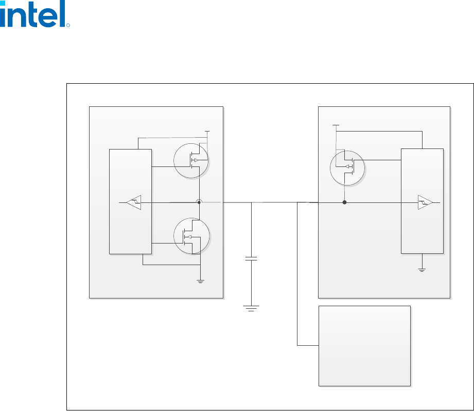
Figure 6. Example for PECI Host-Clients Connection
VCC
ST
Host / Originator
Q1
nX
Q2
1X
PECI
C
PECI
<10pF/Node
Q3
nX
VCC
ST
PECI Client
Additional
PECI Clients
R
12th Generation Intel
®
Core
™
Processors—Technologies
12
th
Generation Intel
®
Core
™
Processors
Datasheet, Volume 1 of 2 February 2023
28 Doc. No.: 655258, Rev.: 010
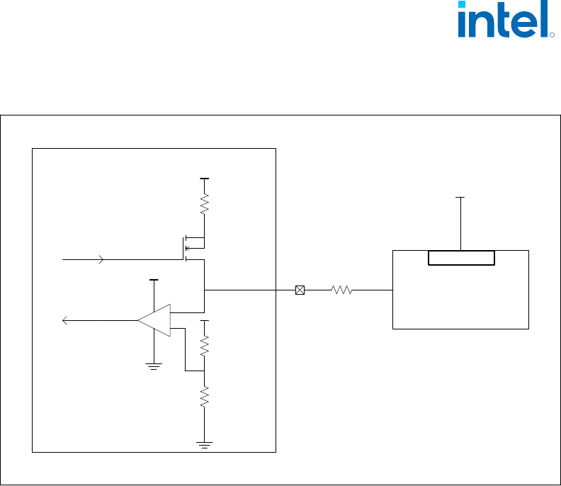
Figure 7. Example for PECI EC Connection
VCCST
VCCST
VCCST
R
In
Out
Processor
PECI
43 Ohm
Embedded
Controller
VCCST
VREF_CPU
Intel
®
Virtualization Technology
Intel
®
Virtualization Technology (Intel
®
VT) makes a single system appear as multiple
independent systems to software. This allows multiple, independent operating systems
to run simultaneously on a single system. Intel
®
VT comprises technology components
to support Virtualization of platforms based on Intel
®
architecture microprocessors
and chipsets.
Intel
®
Virtualization Technology (Intel
®
VT) Intel
®
64 and Intel
®
Architecture (Intel
®
VT-x) added hardware support in the processor to improve the Virtualization
performance and robustness. Intel
®
Virtualization Technology for Directed I/O (Intel
®
VT-d) extends Intel
®
VT-x by adding hardware assisted support to improve I/O device
Virtualization performance.
Intel
®
VT-x specifications and functional descriptions are included in the Intel
®
64
Architectures Software Developer’s Manual, Volume 3. Available at:
http://www.intel.com/products/processor/manuals
The Intel
®
VT-d specification and other VT documents can be referenced at:
http://www.intel.com/content/www/us/en/virtualization/virtualization-technology/.
2.2
R
Technologies—12th Generation Intel
®
Core
™
Processors
12
th
Generation Intel
®
Core
™
Processors
February 2023 Datasheet, Volume 1 of 2
Doc. No.: 655258, Rev.: 010 29

Intel
®
VT for Intel
®
64 and Intel
®
Architecture
Objectives
Intel
®
Virtualization Technology for Intel
®
64 and Intel
®
Architecture (Intel
®
VT-x)
provides hardware acceleration for virtualization of IA platforms. Virtual Machine
Monitor (VMM) can use Intel
®
VT-x features to provide an improved reliable
Virtualization platform. By using Intel
®
VT-x, a VMM is:
• Robust: VMMs no longer need to use para-virtualization or binary translation. This
means that VMMs will be able to run off-the-shelf operating systems and
applications without any special steps.
• Enhanced: Intel
®
VT enables VMMs to run 64-bit guest operating systems on IA
x86 processors.
• More Reliable: Due to the hardware support, VMMs can now be smaller, less
complex, and more efficient. This improves reliability and availability and reduces
the potential for software conflicts.
• More Secure: The use of hardware transitions in the VMM strengthens the
isolation of VMs and further prevents corruption of one VM from affecting others
on the same system.
Key Features
The processor supports the following added new Intel
®
VT-x features:
• Mode-based Execute Control for EPT (MBEC) - A mode of EPT operation which
enables different controls for executability of Guest Physical Address (GPA) based
on Guest specified mode (User/ Supervisor) of linear address translating to the
GPA. When the mode is enabled, the executability of a GPA is defined by two bits
in EPT entry. One bit for accesses to user pages and other one for accesses to
supervisor pages.
— This mode requires changes in VMCS and EPT entries. VMCS includes a bit
"Mode-based execute control for EPT" which is used to enable/disable the
mode. An additional bit in EPT entry is defined as "execute access for user-
mode linear addresses"; the original EPT execute access bit is considered as
"execute access for supervisor-mode linear addresses". If the "mode-based
execute control for EPT" VM-execution control is disabled the additional bit is
ignored and the system work with one bit i.e. the original bit, for execute
control for both user and supervisor pages.
— Behavioral changes - Behavioral changes are across three areas:
• Access to GPA - If the "Mode-based execute control for EPT"
VMexecution control is 1, treatment of guest-physical accesses by
instruction fetches depends on the linear address from which an
instruction is being fetched.
1. If the translation of the linear address specifies user mode (the U/S bit
was set in every paging structure entry used to translate the linear
address), the resulting guest-physical address is executable under EPT
only if the XU bit (at position 10) is set in every EPT paging-structure
entry used to translate the guest-physical address.
2.2.1
R
12th Generation Intel
®
Core
™
Processors—Technologies
12
th
Generation Intel
®
Core
™
Processors
Datasheet, Volume 1 of 2 February 2023
30 Doc. No.: 655258, Rev.: 010

2. If the translation of the linear address specifies supervisor mode (the
U/ S bit was clear in at least one of the paging-structure entries used
to translate the linear address), the resulting guest-physical address is
executable under EPT only if the XS bit is set in every EPT paging-
structure entry used to translate the guest-physical address.
• The XU and XS bits are used only when translating linear addresses for
guest code fetches. They do not apply to guest page walks, data accesses,
or A/D-bit updates.
• VMEntry - If the "activate secondary controls" and "Mode-based execute control
for EPT" VM-execution controls are both 1, VM entries ensure that the "enable
EPT" VM-execution control is 1. VM entry fails if this check fails. When such a
failure occurs, control is passed to the next instruction.
• VMExit - The exit qualification due to EPT violation reports clearly whether the
violation was due to User mode access or supervisor mode access.
— Capability Querying: IA32_VMX_PROCBASED_CTLS2 has bit to indicate the
capability, RDMSR can be used to read and query whether the processor
supports the capability or not.
• Extended Page Table (EPT) Accessed and Dirty Bits
— EPT A/D bits enabled VMMs to efficiently implement memory management and
page classification algorithms to optimize VM memory operations, such as de-
fragmentation, paging, live migration, and check-pointing. Without hardware
support for EPT A/D bits, VMMs may need to emulate A/D bits by marking EPT
paging-structures as not-present or read-only, and incur the overhead of EPT
page-fault VM exits and associated software processing.
• EPTP (EPT pointer) switching
— EPTP switching is a specific VM function. EPTP switching allows guest software
(in VMX non-root operation, supported by EPT) to request a different EPT
paging-structure hierarchy. This is a feature by which software in VMX non-
root operation can request a change of EPTP without a VM exit. The software
will be able to choose among a set of potential EPTP values determined in
advance by software in VMX root operation.
• Pause loop exiting
— Support VMM schedulers seeking to determine when a virtual processor of a
multiprocessor virtual machine is not performing useful work. This situation
may occur when not all virtual processors of the virtual machine are currently
scheduled and when the virtual processor in question is in a loop involving the
PAUSE instruction. The new feature allows detection of such loops and is thus
called PAUSE-loop exiting.
The processor IA core supports the following Intel
®
VT-x features:
• Extended Page Tables (EPT)
— EPT is hardware assisted page table virtualization
— It eliminates VM exits from guest OS to the VMM for shadow page-table
maintenance
• Virtual Processor IDs (VPID)
— Ability to assign a VM ID to tag processor IA core hardware structures (such
as TLBs)
R
Technologies—12th Generation Intel
®
Core
™
Processors
12
th
Generation Intel
®
Core
™
Processors
February 2023 Datasheet, Volume 1 of 2
Doc. No.: 655258, Rev.: 010 31

— This avoids flushes on VM transitions to give a lower-cost VM transition time
and an overall reduction in virtualization overhead.
• Guest Preemption Timer
— The mechanism for a VMM to preempt the execution of a guest OS after an
amount of time specified by the VMM. The VMM sets a timer value before
entering a guest
— The feature aids VMM developers in flexibility and Quality of Service (QoS)
guarantees
• Descriptor-Table Exiting
— Descriptor-table exiting allows a VMM to protect a guest OS from internal
(malicious software based) attack by preventing the relocation of key system
data structures like IDT (interrupt descriptor table), GDT (global descriptor
table), LDT (local descriptor table), and TSS (task segment selector).
— A VMM using this feature can intercept (by a VM exit) attempts to relocate
these data structures and prevent them from being tampered by malicious
software.
Intel
®
Virtualization Technology for Directed I/O
Intel
®
VT-d Objectives
The key Intel
®
Virtualization Technology (Intel
®
VT) for Directed I/O (Intel
®
VT-d)
objectives are domain-based isolation and hardware-based virtualization. A domain
can be abstractly defined as an isolated environment in a platform to which a subset
of host physical memory is allocated. Intel
®
VT-d provides accelerated I/O
performance for a Virtualization platform and provides software with the following
capabilities:
• I/O Device Assignment and Security: for flexibly assigning I/O devices to VMs
and extending the protection and isolation properties of VMs for I/O operations.
• DMA Remapping: for supporting independent address translations for Direct
Memory Accesses (DMA) from devices.
• Interrupt Remapping: for supporting isolation and routing of interrupts from
devices and external interrupt controllers to appropriate VMs.
• Reliability: for recording and reporting to system software DMA and interrupt
errors that may otherwise corrupt memory or impact VM isolation.
Intel
®
VT-d accomplishes address translation by associating transaction from a given
I/O device to a translation table associated with the Guest to which the device is
assigned. It does this by means of the data structure in the following illustration. This
table creates an association between the device's PCI Express* Bus/Device/Function
(B/D/F) number and the base address of a translation table. This data structure is
populated by a VMM to map devices to translation tables in accordance with the device
assignment restrictions above and to include a multi-level translation table (VT-d
Table) that contains Guest specific address translations.
2.2.2
R
12th Generation Intel
®
Core
™
Processors—Technologies
12
th
Generation Intel
®
Core
™
Processors
Datasheet, Volume 1 of 2 February 2023
32 Doc. No.: 655258, Rev.: 010

Figure 8. Device to Domain Mapping Structures
Root entry 0
Root entry N
Root entry 255
Context entry 0
Context entry 255
Context entry 0
Context entry 255
(Bus 255)
(Bus N)
(Bus 0)
Root entry table
(Dev 31, Func 7)
(Dev 0, Func 1)
(Dev 0, Func 0)
Context entry Table
For bus N
Context entry Table
For bus 0
Address Translation
Structures for Domain A
Address Translation
Structures for Domain B
Intel
®
VT-d functionality often referred to as an Intel
®
VT-d Engine, has typically been
implemented at or near a PCI Express* host bridge component of a computer system.
This might be in a chipset component or in the PCI Express functionality of a processor
with integrated I/O. When one such VT-d engine receives a PCI Express transaction
from a PCI Express bus, it uses the B/D/F number associated with the transaction to
search for an Intel
®
VT-d translation table. In doing so, it uses the B/D/F number to
traverse the data structure shown in the above figure. If it finds a valid Intel
®
VT-d
table in this data structure, it uses that table to translate the address provided on the
PCI Express bus. If it does not find a valid translation table for a given translation, this
results in an Intel
®
VT-d fault. If Intel
®
VT-d translation is required, the Intel
®
VT-d
engine performs an N-level table walk.
R
Technologies—12th Generation Intel
®
Core
™
Processors
12
th
Generation Intel
®
Core
™
Processors
February 2023 Datasheet, Volume 1 of 2
Doc. No.: 655258, Rev.: 010 33

For more information, refer to Intel
®
Virtualization Technology for Directed I/O
Architecture Specification http://www.intel.com/content/dam/www/public/us/en/
documents/product-specifications/vt-directed-io-spec.pdf
Intel
®
VT-d Key Features
The processor supports the following Intel
®
VT-d features:
• Memory controller and processor graphics comply with the Intel
®
VT-d 2.1
Specification.
• Two Intel
®
VT-d DMA remap engines.
— iGFX DMA remap engine
— Default DMA remap engine (covers all devices except iGFX)
• Support for root entry, context entry, and the default context
• 46-bit guest physical address and host physical address widths
• Support for 4K page sizes only
• Support for register-based fault recording only (for single entry only) and support
for MSI interrupts for faults
• Support for both leaf and non-leaf caching
• Support for boot protection of default page table
• Support for non-caching of invalid page table entries
• Support for hardware-based flushing of translated but pending writes and pending
reads, on IOTLB invalidation
• Support for Global, Domain-specific and Page specific IOTLB invalidation
• MSI cycles (MemWr to address FEEx_xxxxh) not translated.
• Interrupt Remapping is supported
• Queued invalidation is supported
• Intel
®
VT-d translation bypass address range is supported (Pass Through)
The processor supports the following added new Intel
®
VT-d features:
• 4-level Intel
®
VT-d Page walk – both default Intel
®
VT-d engine, as well as the
Processor Graphics VT-d engine are upgraded to support 4-level Intel
®
VT-d tables
(adjusted guest address width of 48 bits)
• Intel
®
VT-d super-page – support of Intel
®
VT-d super-page (2 MB, 1 GB) for
default Intel
®
VT-d engine (that covers all devices except IGD)
IGD Intel
®
VT-d engine does not support super-page and BIOS should disable
super-page in default Intel
®
VT-d engine when iGfx is enabled.
NOTE
Intel
®
VT-d Technology may not be available on all SKUs.
R
12th Generation Intel
®
Core
™
Processors—Technologies
12
th
Generation Intel
®
Core
™
Processors
Datasheet, Volume 1 of 2 February 2023
34 Doc. No.: 655258, Rev.: 010

Intel
®
APIC Virtualization Technology (Intel
®
APICv)
APIC virtualization is a collection of features that can be used to support the
virtualization of interrupts and the Advanced Programmable Interrupt Controller
(APIC).
When APIC virtualization is enabled, the processor emulates many accesses to the
APIC, tracks the state of the virtual APIC, and delivers virtual interrupts — all in VMX
non-root operation without a VM exit.
The following are the VM-execution controls relevant to APIC virtualization and virtual
interrupts:
• Virtual-interrupt Delivery. This controls enables the evaluation and delivery of
pending virtual interrupts. It also enables the emulation of writes (memory-
mapped or MSR-based, as enabled) to the APIC registers that control interrupt
prioritization.
• Use TPR Shadow. This control enables emulation of accesses to the APIC’s task-
priority register (TPR) via CR8 and, if enabled, via the memory-mapped or MSR-
based interfaces.
• Virtualize APIC Accesses. This control enables virtualization of memory-mapped
accesses to the APIC by causing VM exits on accesses to a VMM-specified APIC-
access page. Some of the other controls, if set, may cause some of these accesses
to be emulated rather than causing VM exits.
• Virtualize x2APIC Mode. This control enables virtualization of MSR-based
accesses to the APIC.
• APIC-register Virtualization. This control allows memory-mapped and MSR-
based reads of most APIC registers (as enabled) by satisfying them from the
virtual-APIC page. It directs memory-mapped writes to the APIC-access page to
the virtual-APIC page, following them by VM exits for VMM emulation.
• Process Posted Interrupts. This control allows software to post virtual
interrupts in a data structure and send a notification to another logical processor;
upon receipt of the notification, the target processor will process the posted
interrupts by copying them into the virtual-APIC page.
NOTE
Intel
®
APIC Virtualization Technology may not be available on all SKUs.
Intel
®
APIC Virtualization specifications and functional descriptions are included in the
Intel
®
64 Architectures Software Developer’s Manual, Volume 3. Available at:
http://www.intel.com/products/processor/manuals
Hypervisor-Managed Linear Address Translation
Hypervisor-Managed Linear Address Translation (HLAT) is active when the “enable
HLAT” VM-execution control is 1. The processor looks up the HLAT if, during a guest
linear address translation, the guest linear address matches the Protected Linear
Range. The lookup from guest linear addresses to the guest physical address and
attributes is determined by a set of HLAT paging structures.
2.2.3
2.2.4
R
Technologies—12th Generation Intel
®
Core
™
Processors
12
th
Generation Intel
®
Core
™
Processors
February 2023 Datasheet, Volume 1 of 2
Doc. No.: 655258, Rev.: 010 35

The guest paging structure managed by the guest OS specifies the ordinary
translation of a guest linear address to the guest physical address and attributes that
the guest ring-0 software has programmed, whereas HLAT specifies the alternate
translation of the guest linear address to guest physical address and attributes that
the Secure Kernel and VMM seek to enforce. A logical processor uses HLAT to translate
guest linear addresses only when those guest linear addresses are used to access
memory (both for code fetch and data load/store) and the guest linear addresses
match the PLR programmed by the VMM/Secure Kernel.
HLAT specifications and functional descriptions are included in the Intel
®
Architecture
Instruction Set Extensions Programming Reference. Available at:
https://software.intel.com/en-us/download/intel-architecture-instruction-set-
extensions-programming-reference
Security Technologies
Intel
®
Trusted Execution Technology
Intel
®
Trusted Execution Technology (Intel
®
TXT) defines platform-level
enhancements that provide the building blocks for creating trusted platforms.
The Intel
®
TXT platform helps to provide the authenticity of the controlling
environment such that those wishing to rely on the platform can make an appropriate
trust decision. The Intel
®
TXT platform determines the identity of the controlling
environment by accurately measuring and verifying the controlling software.
Another aspect of the trust decision is the ability of the platform to resist attempts to
change the controlling environment. The Intel
®
TXT platform will resist attempts by
software processes to change the controlling environment or bypass the bounds set by
the controlling environment.
Intel
®
TXT is a set of extensions designed to provide a measured and controlled
launch of system software that will then establish a protected environment for itself
and any additional software that it may execute.
These extensions enhance two areas:
• The launching of the Measured Launched Environment (MLE).
• The protection of the MLE from potential corruption.
The enhanced platform provides these launch and control interfaces using Safer Mode
Extensions (SMX).
The SMX interface includes the following functions:
• Measured/Verified launch of the MLE.
• Mechanisms to ensure the above measurement is protected and stored in a secure
location.
• Protection mechanisms that allow the MLE to control attempts to modify itself.
The processor also offers additional enhancements to System Management Mode
(SMM) architecture for enhanced security and performance. The processor provides
new MSRs to:
• Enable a second SMM range
2.3
2.3.1
R
12th Generation Intel
®
Core
™
Processors—Technologies
12
th
Generation Intel
®
Core
™
Processors
Datasheet, Volume 1 of 2 February 2023
36 Doc. No.: 655258, Rev.: 010

• Enable SMM code execution range checking
• Select whether SMM Save State is to be written to legacy SMRAM or to MSRs
• Determine if a thread is going to be delayed entering SMM
• Determine if a thread is blocked from entering SMM
• Targeted SMI, enable/disable threads from responding to SMIs, both VLWs, and
IPI
For the above features, BIOS should test the associated capability bit before
attempting to access any of the above registers. The capability bits are discussed in
the register description.
For more information, refer to the Intel
®
Trusted Execution Technology Measured
Launched Environment Programming Guide at:
http://www.intel.com/content/www/us/en/software-developers/intel-txt-software-
development-guide.html.
NOTE
Intel
®
TXT Technology may not be available on all SKUs.
Intel
®
Advanced Encryption Standard New Instructions
The processor supports Intel
®
Advanced Encryption Standard New Instructions (Intel
®
AES-NI) that are a set of Single Instruction Multiple Data (SIMD) instructions that
enable fast and secure data encryption and decryption based on the Advanced
Encryption Standard (AES). Intel
®
AES-NI is valuable for a wide range of
cryptographic applications, such as applications that perform bulk encryption/
decryption, authentication, random number generation, and authenticated encryption.
AES is broadly accepted as the standard for both government and industrial
applications and is widely deployed in various protocols.
Intel
®
AES-NI consists of six Intel
®
SSE instructions. Four instructions, AESENC,
AESENCLAST, AESDEC, and AESDELAST facilitate high-performance AES encryption
and decryption. The other two, AESIMC and AESKEYGENASSIST, support the AES key
expansion procedure. Together, these instructions provide full hardware for supporting
AES; offering security, high performance, and a great deal of flexibility.
This generation of the processor has increased the performance of the Intel
®
AES-NI
significantly compared to previous products.
The Intel
®
AES-NI specifications and functional descriptions are included in the Intel
®
64 Architectures Software Developer’s Manual, Volume 2. Available at:
http://www.intel.com/products/processor/manuals
NOTE
Intel
®
AES-NI Technology may not be available on all SKUs.
2.3.2
R
Technologies—12th Generation Intel
®
Core
™
Processors
12
th
Generation Intel
®
Core
™
Processors
February 2023 Datasheet, Volume 1 of 2
Doc. No.: 655258, Rev.: 010 37

Perform Carry-Less Multiplication Quad Word Instruction
The processor supports the carry-less multiplication instruction, ie, Perform Carry-Less
Multiplication Quad Word Instruction (PCLMULQDQ). PCLMULQDQ is a Single
Instruction Multiple Data (SIMD) instruction that computes the 128-bit carry-less
multiplication of two 64-bit operands without generating and propagating carries.
Carry-less multiplication is an essential processing component of several cryptographic
systems and standards. Hence, accelerating carry-less multiplication can significantly
contribute to achieving high-speed secure computing and communication.
PCLMULQDQ specifications and functional descriptions are included in the Intel
®
64
Architectures Software Developer’s Manual, Volume 2. Available at:
http://www.intel.com/products/processor/manuals
Intel
®
Secure Key
The processor supports Intel
®
Secure Key (formerly known as Digital Random Number
Generator or DRNG), a software visible random number generation mechanism
supported by a high-quality entropy source. This capability is available to
programmers through the RDRAND instruction. The resultant random number
generation capability is designed to comply with existing industry standards in this
regard (ANSI X9.82 and NIST SP 800-90).
Some possible usages of the RDRAND instruction include cryptographic key generation
as used in a variety of applications, including communication, digital signatures,
secure storage, etc.
RDRAND specifications and functional descriptions are included in the Intel
®
64
Architectures Software Developer’s Manual, Volume 2. Available at:
http://www.intel.com/products/processor/manuals
Execute Disable Bit
The Execute Disable Bit allows memory to be marked as non-executable when
combined with a supporting operating system. If code attempts to run in non-
executable memory, the processor raises an error to the operating system. This
feature can prevent some classes of viruses or worms that exploit buffer overrun
vulnerabilities and can, thus, help improve the overall security of the system.
Boot Guard Technology
Boot Guard technology is a part of boot integrity protection technology. Boot Guard
can help protect the platform boot integrity by preventing the execution of
unauthorized boot blocks. With Boot Guard, platform manufacturers can create boot
policies such that invocation of an unauthorized (or untrusted) boot block will trigger
the platform protection per the manufacturer's defined policy.
With verification based in the hardware, Boot Guard extends the trust boundary of the
platform boot process down to the hardware level.
Boot Guard accomplishes this by:
• Providing of hardware-based Static Root of Trust for Measurement (S-RTM) and
the Root of Trust for Verification (RTV) using Intel architectural components.
2.3.3
2.3.4
2.3.5
2.3.6
R
12th Generation Intel
®
Core
™
Processors—Technologies
12
th
Generation Intel
®
Core
™
Processors
Datasheet, Volume 1 of 2 February 2023
38 Doc. No.: 655258, Rev.: 010

• Providing of architectural definition for platform manufacturer Boot Policy.
• Enforcing manufacturer provided Boot Policy using Intel architectural components.
Benefits of this protection are that Boot Guard can help maintain platform integrity by
preventing re-purposing of the manufacturer’s hardware to run an unauthorized
software stack.
NOTE
Boot Guard availability may vary between the different SKUs.
Intel
®
Supervisor Mode Execution Protection
Intel
®
Supervisor Mode Execution Protection (Intel
®
SMEP) is a mechanism that
provides the next level of system protection by blocking malicious software attacks
from user mode code when the system is running in the highest privilege level. This
technology helps to protect from virus attacks and unwanted code from harming the
system. For more information, refer to Intel
®
64 Architectures Software Developer’s
Manual, Volume 3 at:
http://www.intel.com/products/processor/manuals
Intel
®
Supervisor Mode Access Protection
Intel
®
Supervisor Mode Access Protection (Intel
®
SMAP) is a mechanism that provides
next level of system protection by blocking a malicious user from tricking the
operating system into branching off user data. This technology shuts down very
popular attack vectors against operating systems.
For more information, refer to the Intel
®
64 Architectures Software Developer’s
Manual, Volume 3:
http://www.intel.com/products/processor/manuals
Intel
®
Secure Hash Algorithm Extensions
The Intel
®
Secure Hash Algorithm Extensions (Intel
®
SHA Extensions) is one of the
most commonly employed cryptographic algorithms. Primary usages of SHA include
data integrity, message authentication, digital signatures, and data de-duplication. As
the pervasive use of security solutions continues to grow, SHA can be seen in more
applications now than ever. The Intel
®
SHA Extensions are designed to improve the
performance of these compute-intensive algorithms on Intel
®
architecture-based
processors.
The Intel
®
SHA Extensions are a family of seven instructions based on the Intel
®
Streaming SIMD Extensions (Intel
®
SSE) that are used together to accelerate the
performance of processing SHA-1 and SHA-256 on Intel architecture-based
processors. Given the growing importance of SHA in our everyday computing devices,
the new instructions are designed to provide a needed boost of performance to
hashing a single buffer of data. The performance benefits will not only help improve
responsiveness and lower power consumption for a given application, but they may
also enable developers to adopt SHA in new applications to protect data while
delivering to their user experience goals. The instructions are defined in a way that
simplifies their mapping into the algorithm processing flow of most software libraries,
thus enabling easier development.
2.3.7
2.3.8
2.3.9
R
Technologies—12th Generation Intel
®
Core
™
Processors
12
th
Generation Intel
®
Core
™
Processors
February 2023 Datasheet, Volume 1 of 2
Doc. No.: 655258, Rev.: 010 39

More information on Intel
®
SHA can be found at:
http://software.intel.com/en-us/artTGLes/intel-sha-extensions
User Mode Instruction Prevention
User Mode Instruction Prevention (UMIP) provides additional hardening capability to
the OS kernel by allowing certain instructions to execute only in supervisor mode
(Ring 0).
If the OS opt-in to use UMIP, the following instruction are enforced to run in supervisor
mode:
• SGDT - Store the GDTR register value
• SIDT - Store the IDTR register value
• SLDT - Store the LDTR register value
• SMSW - Store Machine Status Word
• STR - Store the TR register value
An attempt at such execution in user mode causes a general protection exception
(#GP).
UMIP specifications and functional descriptions are included in the Intel
®
64
Architectures Software Developer’s Manual, Volume 3. Available at:
http://www.intel.com/products/processor/manuals
Read Processor ID
A companion instruction that returns the current logical processor's ID and provides a
faster alternative to using the RDTSCP instruction.
Read Processor ID (RDPID) specifications and functional descriptions are included in
the Intel
®
64 Architectures Software Developer’s Manual, Volume 2. Available at:
http://www.intel.com/products/processor/manuals
Intel
®
Total Memory Encryption - Multi-Key
This technology encrypts the platform's entire memory with multiple encryption keys.
Intel
®
Total Memory Encryption (Intel
®
TME), when enabled via BIOS configuration,
ensures that all memory accessed from the Intel processor is encrypted.
Intel TME encrypts memory accesses using the AES XTS algorithm with 128-bit keys.
The global encryption key used for memory encryption is generated using a hardened
random number generator in the processor and is not exposed to software.
Software (OS/VMM) manages the use of keys and can use each of the available keys
for encrypting any page of the memory. Thus, Intel
®
Total Memory Encryption - Multi-
key (Intel
®
TME-MK) allows page granular encryption of memory. By default Intel
TME-MK uses the Intel TME encryption key unless explicitly specified by software.
2.3.10
2.3.11
2.3.12
R
12th Generation Intel
®
Core
™
Processors—Technologies
12
th
Generation Intel
®
Core
™
Processors
Datasheet, Volume 1 of 2 February 2023
40 Doc. No.: 655258, Rev.: 010

Data in-memory and on the external memory buses is encrypted and exists in plain
text only inside the processor. This allows existing software to operate without any
modification while protecting memory using Intel TME. Intel TME does not protect
memory from modifications.
Intel TME allows the BIOS to specify a physical address range to remain unencrypted.
Software running on Intel TME enabled system has full visibility into all portions of
memory that are configured to be unencrypted by reading a configuration register in
the processor.
NOTES
• Memory access to nonvolatile memory (Intel
®
Optane
™
) is encrypted as well.
• More information on Intel TME-MK can be found at:
https://software.intel.com/sites/default/files/managed/a5/16/Total-Memory-
Encryption-Multi-Key-Spec.pdf
• A cold boot is required when enable/ disable Intel TME feature on this platform.
Intel
®
Control-flow Enforcement Technology
Return-oriented Programming (ROP), and similarly CALL/JMP-oriented programming
(COP/JOP), have been the prevalent attack methodology for stealth exploit writers
targeting vulnerabilities in programs.
Intel
®
Control-flow Enforcement Technology (Intel
®
CET) provides the following
components to defend against ROP/JOP style control-flow subversion attacks:
Shadow Stack
A shadow stack is a second stack for the program that is used exclusively for control
transfer operations. This stack is separate from the data stack and can be enabled for
operation individually in user mode or supervisor mode.
The shadow stack is protected from tamper through the page table protections such
that regular store instructions cannot modify the contents of the shadow stack. To
provide this protection the page table protections are extended to support an
additional attribute for pages to mark them as “Shadow Stack” pages. When shadow
stacks are enabled, control transfer instructions/flows such as near call, far call, call to
interrupt/exception handlers, etc. store their return addresses to the shadow stack.
The RET instruction pops the return address from both stacks and compares them. If
the return addresses from the two stacks do not match, the processor signals a
control protection exception (#CP). Stores from instructions such as MOV, XSAVE, etc.
are not allowed to the shadow stack.
Indirect Branch Tracking
The ENDBR32 and ENDBR64 (collectively ENDBRANCH) are two new instructions that
are used to mark valid indirect CALL/JMP target locations in the program. This
instruction is a NOP on legacy processors for backward compatibility.
The processor implements a state machine that tracks indirect JMP and CALL
instructions. When one of these instructions is seen, the state machine moves from
IDLE to WAIT_FOR_ENDBRANCH state. In WAIT_FOR_ENDBRANCH state the next
2.3.13
2.3.13.1
2.3.13.2
R
Technologies—12th Generation Intel
®
Core
™
Processors
12
th
Generation Intel
®
Core
™
Processors
February 2023 Datasheet, Volume 1 of 2
Doc. No.: 655258, Rev.: 010 41

instruction in the program stream must be an ENDBRANCH. If an ENDBRANCH is not
seen the processor causes a control protection fault (#CP), otherwise the state
machine moves back to IDLE state.
More information on Intel
®
CET can be found at:
https://software.intel.com/sites/default/files/managed/4d/2a/control-flow-
enforcement-technology-preview.pdf
KeyLocker Technology
A method to make long-term keys short-lived without exposing them. This protects
against vulnerabilities when keys can be exploited and used to attack encrypted data
such as disk drives.
An instruction (LOADIWKEY) allows the OS to load a random wrapping value (IWKey).
The IWKey can be backed up and restored by the OS to/from the PCH in a secure
manner.
The Software can wrap it own key via the ENCODEKEY instruction and receive a
handle. The handle is used with the AES*KL instructions to handle encrypt and
decrypt operations. Once a handle is obtained, the software can delete the original key
from memory.
Devil’s Gate Rock
Devil’s Gate Rock (DGR) is a BIOS hardening technology that splits SMI (System
Management Interrupts) handlers into Ring 3 and Ring 0 portions.
Supervisor/user paging on the smaller Ring 0 portion will enforce access policy for all
the ring 3 code with regard to the SMM state save, MSR registers, IO ports and other
registers.
The Ring 0 portion can perform save/restore of register context to allow the Ring 3
section to make use of those registers without having access to the OS context or the
ability to modify the OS context.
The Ring 0 portion is signed and provided by Intel. This portion is attested by the
processor.
Power and Performance Technologies
Intel
®
Smart Cache Technology
The Intel
®
Smart Cache Technology is a shared Last Level Cache (LLC).
• The LLC is non-inclusive.
• The LLC may also be referred to as a 3rd level cache.
• The LLC is shared between all IA cores as well as the Processor Graphics.
• For P Cores The 1st and 2nd level caches are not shared between physical cores
and each physical core has a separate set of caches.
• For E Cores The 1st level cache is not shared between physical cores and each
physical core has a separate set of caches.
2.3.14
2.3.15
2.4
2.4.1
R
12th Generation Intel
®
Core
™
Processors—Technologies
12
th
Generation Intel
®
Core
™
Processors
Datasheet, Volume 1 of 2 February 2023
42 Doc. No.: 655258, Rev.: 010
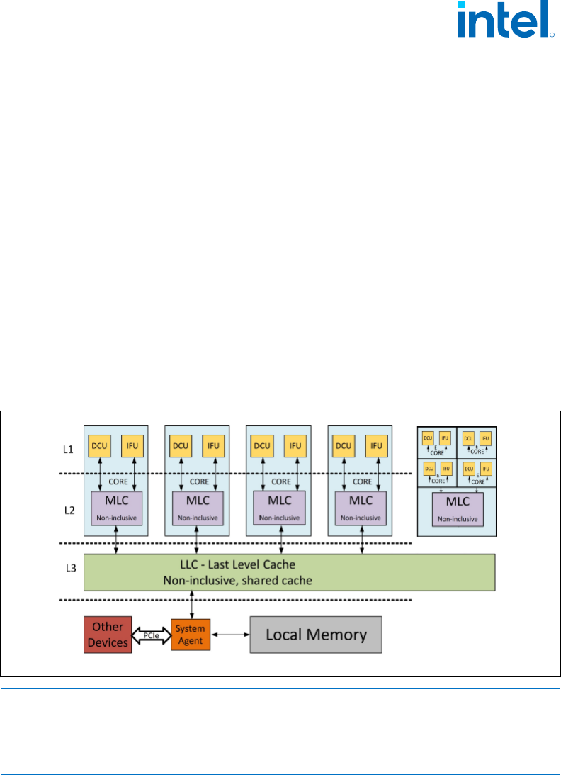
• For E Cores The 2nd level cache is shared between 4 physical cores.
• The size of the LLC is SKU specific with a maximum of 3MB per P physical core or
4 E cores and is a 12-way associative cache.
IA Cores Level 1 and Level 2 Caches
P Cores 1st level cache is divided into a data cache (DFU) and an instruction cache
(IFU). The processor 1st level cache size is 48KB for data and 32KB for instructions.
The 1st level cache is an 12-way associative cache.
E Cores 1st level cache is divided into a data cache (DFU) and an instruction cache
(IFU). The processor 1st level cache size is 32KB for data and 64KB for instructions.
The 1st level cache is an 8-way associative cache.
The 2nd level cache holds both data and instructions. It is also referred to as mid-level
cache or MLC. The P Cores 2nd level cache size is 1.25MB and is a 10-way non-
inclusive associative cache., 4 E Cores processors share 2MB 2nd level cache and is a
16-way non-inclusive. associative cache.
Figure 9. Hybrid Cache
NOTES
1. L1 Data cache (DCU) - 48KB (P-core) - 32KB (E-Core)
2. L1 Instruction cache (IFU) - 32KB (P-Core) - 64KB (E-Core)
3. MLC - Mid Level Cache - 1.25MB (P-Core) - 2MB (shared by 4 E-Cores)
Ring Interconnect
The Ring is a high speed, wide interconnect that links the processor cores, processor
graphics and the System Agent.
The Ring shares frequency and voltage with the Last Level Cache (LLC).
The Ring's frequency dynamically changes. Its frequency is relative to both processor
cores and processor graphics frequencies.
2.4.2
2.4.3
R
Technologies—12th Generation Intel
®
Core
™
Processors
12
th
Generation Intel
®
Core
™
Processors
February 2023 Datasheet, Volume 1 of 2
Doc. No.: 655258, Rev.: 010 43

Intel
®
Performance Hybrid Architecture
The processor contains two types of cores, denoted as P-Cores and E-Cores (P core is
a Performance core and E core is efficient core ).
The P-Cores and E-Cores share the same instruction set.
The available instruction sets, when hybrid computing is enabled, is limited compared
to the instruction sets available to P-Cores.
P core and E core frequency's will be determined by the processor algorithmic, to
maximize performance and power optimization.
The following instruction sets are available only when the P-Core are enabled:
• FP16 support
For more details, refer to: https://www.intel.com/content/www/us/en/developer/
articles/technical/hybrid-architecture.html
NOTE
Hybrid Computing may not be available on all SKUs.
Intel
®
Turbo Boost Max Technology 3.0
The Intel
®
Turbo Boost Max Technology 3.0 (ITBMT 3.0) grants a different maximum
Turbo frequency for individual processor cores.
To enable ITBMT 3.0 the processor exposes individual core capabilities; including
diverse maximum turbo frequencies.
An operating system that allows for varied per core frequency capability can then
maximize power savings and performance usage by assigning tasks to the faster
cores, especially on low core count workloads.
Processors enabled with these capabilities can also allow software (most commonly a
driver) to override the maximum per-core Turbo frequency limit and notify the
operating system via an interrupt mechanism.
For more information on the Intel
®
Turbo Boost Max 3.0 Technology, refer to http://
www.intel.com/content/www/us/en/architecture-and-technology/turbo-boost/turbo-
boost-max-technology.html
NOTE
Intel
®
Turbo Boost Max 3.0 Technology may not be available on all SKUs.
Intel
®
Hyper-Threading Technology
The processor supports Intel
®
Hyper-Threading Technology (Intel
®
HT Technology)
that allows an execution processor IA core to function as two logical processors. While
some execution resources such as caches, execution units, and buses are shared,
each logical processor has its own architectural state with its own set of general-
purpose registers and control registers. This feature should be enabled using the BIOS
and requires operating system support.
2.4.4
2.4.5
2.4.6
R
12th Generation Intel
®
Core
™
Processors—Technologies
12
th
Generation Intel
®
Core
™
Processors
Datasheet, Volume 1 of 2 February 2023
44 Doc. No.: 655258, Rev.: 010

Intel recommends enabling Intel
®
Hyper-Threading Technology with Microsoft*
Windows* 7 or newer and disabling Intel
®
Hyper-Threading Technology using the
BIOS for all previous versions of Windows* operating systems.
NOTE
Intel
®
HT Technology may not be available on all SKUs.
Intel
®
Turbo Boost Technology 2.0
The Intel
®
Turbo Boost Technology 2.0 allows the processor IA core/processor
graphics core to opportunistically and automatically run faster than the processor IA
core base frequency/processor graphics base frequency if it is operating below power,
temperature, and current limits. The Intel
®
Turbo Boost Technology 2.0 feature is
designed to increase the performance of both multi-threaded and single-threaded
workloads.
Compared with previous generation products, Intel
®
Turbo Boost Technology 2.0 will
increase the ratio of application power towards Processor Base Power (a.k.a TDP) and
also allows to increase power above Processor Base Power (a.k.a TDP) as high as PL2
for short periods of time. Thus, thermal solutions and platform cooling that are
designed to less than thermal design guidance might experience thermal and
performance issues since more applications will tend to run at the maximum power
limit for significant periods of time.
NOTE
Intel
®
Turbo Boost Technology 2.0 may not be available on all SKUs.
Intel
®
Turbo Boost Technology 2.0 Power Monitoring
When operating in turbo mode, the processor monitors its own power and adjusts the
processor and graphics frequencies to maintain the average power within limits over a
thermally significant time period. The processor estimates the package power for all
components on the package. In the event that a workload causes the temperature to
exceed program temperature limits, the processor will protect itself using the Adaptive
Thermal Monitor.
Intel
®
Turbo Boost Technology 2.0 Power Control
Illustration of Intel
®
Turbo Boost Technology 2.0 power control is shown in the
following sections and figures. Multiple controls operate simultaneously allowing
customization for multiple systems thermal and power limitations. These controls
allow for turbo optimizations within system constraints and are accessible using MSR,
MMIO, and PECI interfaces.
Intel
®
Turbo Boost Technology 2.0 Frequency
To determine the highest performance frequency amongst active processor IA cores,
the processor takes the following into consideration:
• The number of processor IA cores operating in the C0 state.
• The estimated processor IA core current consumption and ICCMax settings.
2.4.7
2.4.7.1
2.4.7.2
2.4.7.3
R
Technologies—12th Generation Intel
®
Core
™
Processors
12
th
Generation Intel
®
Core
™
Processors
February 2023 Datasheet, Volume 1 of 2
Doc. No.: 655258, Rev.: 010 45

• The estimated package prior and present power consumption and turbo power
limits.
• The package temperature.
Any of these factors can affect the maximum frequency for a given workload. If the
power, current, or thermal limit is reached, the processor will automatically reduce the
frequency to stay within its Processor Base Power (a.k.a TDP) limit. Turbo processor
frequencies are only active if the operating system is requesting the P0 state. For
more information on P-states and C-states, refer to Power Management on page 58.
Enhanced Intel SpeedStep
®
Technology
Enhanced Intel SpeedStep
®
Technology enables OS to control and select P-state. The
following are the key features of Enhanced Intel SpeedStep
®
Technology:
• Multiple frequencies and voltage points for optimal performance and power
efficiency. These operating points are known as P-states.
• Frequency selection is software controlled by writing to processor MSRs. The
voltage is optimized based on the selected frequency and the number of active
processors IA cores.
— Once the voltage is established, the PLL locks on to the target frequency.
— All active processor IA cores share the same frequency and voltage. In a
multi-core processor, the highest frequency P-state requested among all active
IA cores is selected.
— Software-requested transitions are accepted at any time. If a previous
transition is in progress, the new transition is deferred until the previous
transition is completed.
• The processor controls voltage ramp rates internally to ensure glitch-free
transitions.
NOTE
Because there is low transition latency between P-states, a significant number of
transitions per-second are possible.
Intel
®
Thermal Velocity Boost (Intel
®
TVB)
Intel
®
Thermal Velocity Boost allows the processor IA core to opportunistically and
automatically increase the Intel
®
Turbo Boost Technology 2.0 frequency speed bins
whenever processor temperature and voltage allows.
The Intel
®
Thermal Velocity Boost feature is designed to increase performance of both
multi-threaded and singlethreaded workloads.
NOTE
Intel
®
Thermal Velocity Boost (Intel
®
TVB) may not be available on all SKUs.
2.4.8
2.4.9
R
12th Generation Intel
®
Core
™
Processors—Technologies
12
th
Generation Intel
®
Core
™
Processors
Datasheet, Volume 1 of 2 February 2023
46 Doc. No.: 655258, Rev.: 010

Intel
®
Speed Shift Technology
Intel
®
Speed Shift Technology is an energy efficient method of frequency control by
the hardware rather than relying on OS control. OS is aware of available hardware P-
states and requests the desired P-state or it can let the hardware determine the P-
state. The OS request is based on its workload requirements and awareness of
processor capabilities. Processor decision is based on the different system constraints
for example Workload demand, thermal limits while taking into consideration the
minimum and maximum levels and activity window of performance requested by the
Operating System.
Intel
®
Advanced Vector Extensions 2 (Intel
®
AVX2)
Intel
®
Advanced Vector Extensions 2.0 (Intel
®
AVX2) is the latest expansion of the
Intel instruction set. Intel
®
AVX2 extends the Intel
®
Advanced Vector Extensions
(Intel
®
AVX) with 256-bit integer instructions, floating-point fused multiply-add (FMA)
instructions, and gather operations. The 256-bit integer vectors benefit math, codec,
image, and digital signal processing software. FMA improves performance in face
detection, professional imaging, and high-performance computing. Gather operations
increase vectorization opportunities for many applications. In addition to the vector
extensions, this generation of Intel processors adds new bit manipulation instructions
useful in compression, encryption, and general purpose software. For more
information on Intel
®
AVX, refer to http://www.intel.com/software/avx
Intel
®
Advanced Vector Extensions (Intel
®
AVX) are designed to achieve higher
throughput to certain integer and floating point operation. Due to varying processor
power characteristics, utilizing AVX instructions may cause a) parts to operate below
the base frequency b) some parts with Intel
®
Turbo Boost Technology 2.0 to not
achieve any or maximum turbo frequencies. Performance varies depending on
hardware, software and system configuration and you should consult your system
manufacturer for more information.
Intel
®
Advanced Vector Extensions refers to Intel
®
AVX or Intel
®
AVX2 .
For more information on Intel
®
AVX, refer to https://software.intel.com/en-us/isa-
extensions/intel-avx.
NOTE
Intel
®
AVX and AVX2 Technologies may not be available on all SKUs.
Intel
®
AVX2 Vector Neural Network Instructions (AVX2 VNNI)
Vector instructions for deep learning extension for AVX2.
NOTE
Intel
®
AVX and AVX2 Technologies may not be available on all SKUs.
Intel
®
64 Architecture x2APIC
The x2APIC architecture extends the xAPIC architecture that provides key
mechanisms for interrupt delivery. This extension is primarily intended to increase
processor addressability.
2.4.10
2.4.11
2.4.11.1
2.4.12
R
Technologies—12th Generation Intel
®
Core
™
Processors
12
th
Generation Intel
®
Core
™
Processors
February 2023 Datasheet, Volume 1 of 2
Doc. No.: 655258, Rev.: 010 47

Specifically, x2APIC:
• Retains all key elements of compatibility to the xAPIC architecture:
— Delivery modes
— Interrupt and processor priorities
— Interrupt sources
— Interrupt destination types
• Provides extensions to scale processor addressability for both the logical and
physical destination modes
• Adds new features to enhance the performance of interrupt delivery
• Reduces the complexity of logical destination mode interrupt delivery on link
based architectures
The key enhancements provided by the x2APIC architecture over xAPIC are the
following:
• Support for two modes of operation to provide backward compatibility and
extensibility for future platform innovations:
— In xAPIC compatibility mode, APIC registers are accessed through memory
mapped interface to a 4K-Byte page, identical to the xAPIC architecture.
— In the x2APIC mode, APIC registers are accessed through the Model Specific
Register (MSR) interfaces. In this mode, the x2APIC architecture provides
significantly increased processor addressability and some enhancements on
interrupt delivery.
• Increased range of processor addressability in x2APIC mode:
— Physical xAPIC ID field increases from 8 bits to 32 bits, allowing for interrupt
processor addressability up to 4G-1 processors in physical destination mode. A
processor implementation of x2APIC architecture can support fewer than 32-
bits in a software transparent fashion.
— Logical xAPIC ID field increases from 8 bits to 32 bits. The 32-bit logical
x2APIC ID is partitioned into two sub-fields – a 16-bit cluster ID and a 16-bit
logical ID within the cluster. Consequently, ((2^20) - 16) processors can be
addressed in logical destination mode. Processor implementations can support
fewer than 16 bits in the cluster ID sub-field and logical ID sub-field in a
software agnostic fashion.
• More efficient MSR interface to access APIC registers:
— To enhance inter-processor and self-directed interrupt delivery as well as the
ability to virtualize the local APIC, the APIC register set can be accessed only
through MSR-based interfaces in x2APIC mode. The Memory Mapped IO
(MMIO) interface used by xAPIC is not supported in x2APIC mode.
• The semantics for accessing APIC registers have been revised to simplify the
programming of frequently-used APIC registers by system software. Specifically,
the software semantics for using the Interrupt Command Register (ICR) and End
Of Interrupt (EOI) registers have been modified to allow for more efficient delivery
and dispatching of interrupts.
• The x2APIC extensions are made available to system software by enabling the
local x2APIC unit in the “x2APIC” mode. To benefit from x2APIC capabilities, a new
operating system and a new BIOS are both needed, with special support for the
x2APIC mode.
R
12th Generation Intel
®
Core
™
Processors—Technologies
12
th
Generation Intel
®
Core
™
Processors
Datasheet, Volume 1 of 2 February 2023
48 Doc. No.: 655258, Rev.: 010

• The x2APIC architecture provides backward compatibility to the xAPIC architecture
and forwards extensible for future Intel platform innovations.
NOTE
Intel
®
x2APIC Technology may not be available on all SKUs.
For more information, refer to the Intel
®
64 Architecture x2APIC Specification at
http://www.intel.com/products/processor/manuals/
Intel
®
Dynamic Tuning Technology
Intel
®
Dynamic Tuning (Intel
®
DTT) consists of a set of software drivers and
applications that allow a system manufacturer to optimize system performance and
usability by:
• Dynamically optimize turbo settings of IA processors, power and thermal states of
the platform for optimal performance
• Dynamically adjust the processor’s peak power based on the current power
delivery capability for optimal system usability
• Dynamically mitigate radio frequency interference for better RF throughput.
Intel
®
GMM and Neural Network Accelerator
GNA stands for
Gaussian Mixture Model and Neural Network Accelerator.
The GNA is used to process speech recognition without user training sequence. The
GNA is designed to unload the processor cores and the system memory with complex
speech recognition tasks and improve the speech recognition accuracy. The GNA is
designed to compute millions of Gaussian probability density functions per second
without loading the processor cores while maintaining low power consumption.
2.4.13
2.4.14
R
Technologies—12th Generation Intel
®
Core
™
Processors
12
th
Generation Intel
®
Core
™
Processors
February 2023 Datasheet, Volume 1 of 2
Doc. No.: 655258, Rev.: 010 49
CPU
Core0
CPU
Core2
SRAM GNA
DSP
Memory Bus
DRAM
Memory Bus
CPU
Core3
CPU
Core1
Cache Line Write Back
Writes back to memory the cache line (if dirty) that contains the linear address
specified with the memory operand from any level of the cache hierarchy in the cache
coherence domain. The line may be retained in the cache hierarchy in the non-
modified state. Retaining the line in the cache hierarchy is a performance optimization
2.4.15
R
12th Generation Intel
®
Core
™
Processors—Technologies
12
th
Generation Intel
®
Core
™
Processors
Datasheet, Volume 1 of 2 February 2023
50 Doc. No.: 655258, Rev.: 010

(treated as a hint by hardware) to reduce the possibility of a cache miss on a
subsequent access. Hardware may choose to retain the line at any of the levels in the
cache hierarchy, and in some cases, may invalidate the line from the cache hierarchy.
The source operand is a byte memory location.
The Cache Line Write Back (CLWB) instruction is documented in the Intel
®
Architecture Instruction Set Extensions Programming Reference (future architectures):
https://software.intel.com/sites/default/files/managed/b4/3a/319433-024.pdf
Remote Action Request
Remote Action Request (RAR) enables a significant speed up of several inter-processor
operations by moving such operations from software (OS or application) to hardware.
The main feature is the speedup of TLB shootdowns.
A single RAR operation can invalidate multiple memory pages in the TLB.
A TLB (Translation Lookaside Buffer) is a per-core cache that holds mappings from
virtual to physical addresses.
A TLB shootdown is the process of propagating a change in memory mapping (page
table entry) to all the cores.
RAR supports the following operations:
• Page Invalidation: imitates the operation of performing INVLPG instructions
corresponding or the TLB invalidation corresponding with “MOV CR3 / CR0”
• Page Invalidation without CR3 Match: identical to “Page invalidation”, except
that the processor does not check for a CR3 match
• PCID Invalidation: imitates the operation of performing INVPCID instructions
• EPT Invalidation: imitates the operation of performing INVEPT instructions
• VPID Invalidation: imitates the operation of performing INVVPID instructions
• MSR Write: imitates the operation of WRMSR instructions on all cores
User Mode Wait Instructions
The UMONITOR and UMWAIT are user mode (Ring 3) instructions similar to the
supervisor mode (Ring 0) MONITOR/MWAIT instructions without the C-state
management capability.
TPAUSE us an enhanced PAUSE instruction.
The mnemonics for the three new instructions are:
• UMONITOR: operates just like MONITOR but allowed in all rings.
• UMWAIT: allowed in all rings, and no specification of target C-state.
• TPAUSE: similar to PAUSE but with a software-specified delay. Commonly used in
spin loops.
2.4.16
2.4.17
R
Technologies—12th Generation Intel
®
Core
™
Processors
12
th
Generation Intel
®
Core
™
Processors
February 2023 Datasheet, Volume 1 of 2
Doc. No.: 655258, Rev.: 010 51
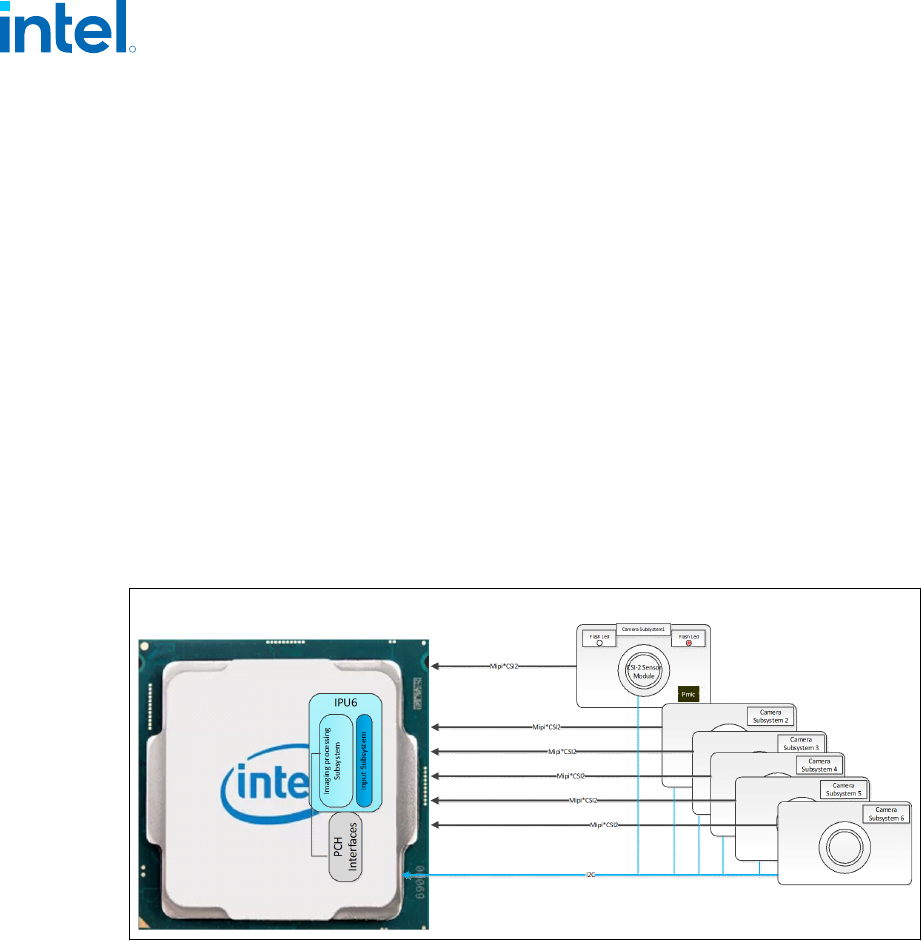
Intel
®
Image Processing Unit
Platform Imaging Infrastructure
The platform imaging infrastructure is based on the following hardware components:
• Camera Subsystem: Located in the lid of the system and contains CMOS sensor,
flash, LED, I/O interface (MIPI* CSI-2 and I2C*), focus control and other
components.
• Camera I/O Controller: The I/O controller is located in the processor and
contains a MIPI-CSI2 host controller. The host controller is a PCI device
(independent of the IPU device). The CSI-2 HCI brings imaging data from an
external image into the system and provides a command and control channel for
the image using I
2
C.
• Intel
®
IPU (Image Processing Unit): The IPU processes raw images captured
by Bayer sensors. The result images are used by still photography and video
capture applications (JPEG, H.264, and so on.).
Figure 10. Processor Camera System
Intel
®
Image Processing Unit
IPU6 is Intel's 6th generation solution for an Imaging Processing Unit, providing
advanced imaging functionality for Intel
®
Core
™
branded processors, as well as more
specialized functionality for High Performance Mobile Phones, Automotive, Digital
Surveillance Systems (DSS), and other market segments.
IPU6 is a continuing evolution of the architecture introduced in IPU4 and enhanced in
IPU5. Additional image quality improvements are introduced, as well as hardware
accelerated support for temporal de-noising and new sensor technologies such as
Spatially Variant Exposure HDR and Dual Photo Diode, among others.
IPU6 provides a complete high quality hardware accelerated pipeline, and is therefore
not dependent on algorithms running on the vector processors to provide the highest
quality output.
• H/P/U - Processor Lines has the most advance IPU6
2.5
2.5.1
2.5.2
R
12th Generation Intel
®
Core
™
Processors—Technologies
12
th
Generation Intel
®
Core
™
Processors
Datasheet, Volume 1 of 2 February 2023
52 Doc. No.: 655258, Rev.: 010

• S/HX - Processor Lines has a lighter version of the IPU.
Debug Technologies
Intel
®
Processor Trace
Intel
®
Processor Trace (Intel
®
PT) is a tracing capability added to Intel
®
Architecture,
for use in software debug and profiling. Intel
®
PT provides the capability for more
precise software control flow and timing information, with limited impact on software
execution. This provides an enhanced ability to debug software crashes, hangs, or
other anomalies, as well as responsiveness and short-duration performance issues.
Intel
®
VTune
™
Amplifier for Systems and the Intel
®
System Debugger are part of
Intel
®
System Studio 2015 (and newer) product, which includes updates for the new
debug and trace features, including Intel
®
PT and Intel
®
Trace Hub.
Intel
®
System Studio 2015 is available for download at https://software.intel.com/en-
us/system-studio.
An update to the Linux* performance utility, with support for Intel
®
PT, is available for
download at https://github.com/virtuoso/linux-perf/tree/intel_pt. It requires
rebuilding the kernel and the perf utility.
Platform CrashLog
• The CrashLog feature is intended for use by system builders (OEMs) as a means to
triage and perform first level debug of failures.
• CrashLog enables the BIOS or the OS to collect data on failures with the intent to
collect and classify the data as well as analyze failure trends.
• CrashLog is a mechanism to collect debug information into a single location and
then allow access to that data via multiple methods, including the BIOS and OS of
the failing system.
• CrashLog is initiated by a Crash Data Detector on observation of error conditions
(TCO watchdog timeout, machine check exceptions, etc.).
• Crash Data Detector notifies the Crash Data Requester of the error condition in
order for the Crash Data Requester to collect Crash Data from several different IPs
and/or Crash Nodes and stores the data to the Crash Data Storage (on-die SRAM)
prior to the reset.
• After the system has rebooted, the Crash Data Collector reads the Crash Data
from the Crash Data Storage and makes the data available to either to software
and/or back to a central server to track error frequency and trends.
Telemetry Aggregator
The Telemetry Aggregator serves as an architectural and discoverable interface to
hardware telemetry:
• Standardized PCIe discovery solution that enables software to discover and
manage telemetry across products
• Standardized definitions for telemetry decode, including data type definitions
2.6
2.6.1
2.6.2
2.6.3
R
Technologies—12th Generation Intel
®
Core
™
Processors
12
th
Generation Intel
®
Core
™
Processors
February 2023 Datasheet, Volume 1 of 2
Doc. No.: 655258, Rev.: 010 53
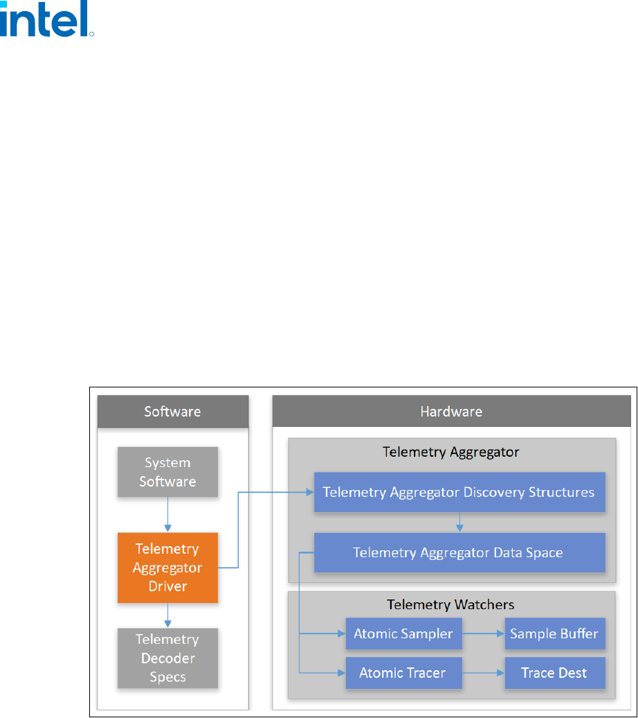
• Exposure of commonly used telemetry for power and performance debug
including:
— P-State status, residency and counters
— C-State status, residency and counters
— Energy monitoring
— Device state monitoring (for example, PCIe L1)
— Interconnect/bus bandwidth counters
— Thermal monitoring
Exposure of SoC state snapshot for atomic monitoring of package power states,
uninterrupted by software that reads.
The Telemetry Aggregator is also a companion to the CrashLog feature where data is
captured about the SoC at the point of a crash. These counters can provide insights
into the nature of the crash.
Figure 11. Telemetry Aggregator
Clock Topology
The processor has 3 reference clocks that drive the various components within the
SoC:
• Processor reference clock or base clock (BCLK). 100MHz with SSC.
• PCIe reference clock (PCTGLK). 100MHz with SSC.
• Fixed clock. 38.4MHz without SSC (crystal clock).
BCLK drives the following clock domains:
• Core
2.7
R
12th Generation Intel
®
Core
™
Processors—Technologies
12
th
Generation Intel
®
Core
™
Processors
Datasheet, Volume 1 of 2 February 2023
54 Doc. No.: 655258, Rev.: 010

• Ring
• Graphics (GT)
• Memory Controller (MC)
• System Agent (SA)
PCTGLK drives the following clock domains:
• PCIe Controller(s)
• DMI/OPIO
Fixed clock drives the following clock domains:
• Display
• SVID controller
• Time Stamp Counters (TSC)
• Type C subsystem
Integrated Reference Clock PLL
The processor includes a phase lock loop (PLL) that generates the reference clock for
the processor from a fixed crystal clock. The processor reference clock is also referred
to as Base Clock or BCLK.
By integrating the BCLK PLL into the processor die, a cleaner clock is achieved at a
lower power compared to the legacy PCH BCLK PLL solution.
The BCLK PLL has controls for RFI/EMI mitigations as well as Overclocking capabilities.
Intel Volume Management Device Technology
Objective
Standard Operating Systems generally recognize individual PCIe Devices and load
individual drivers. This is undesirable in some cases such as, for example, when there
are several PCIe-based hard-drives connected to a platform where the user wishes to
configure them as part of a RAID array. The Operating System current treats
individual hard-drives as separate volumes and not part of a single volume.
In other words, the Operating System requires multiple PCIe devices to have multiple
driver instances, making volume management across multiple host bus adapters
(HBAs) and driver instances difficult.
Intel Volume Management Device (VMD) technology provides a means to provide
volume management across separate PCI Express HBAs and SSDs without requiring
operating system support or communication between drivers. For example, the OS will
see a single RAID volume instead of multiple storage volumes, when Volume
Management Device is used.
Overview
Intel Volume Management Device technology does this by obscuring each storage
controller from the OS, while allowing a single driver to be loaded that would control
each storage controller.
2.7.1
2.8
R
Technologies—12th Generation Intel
®
Core
™
Processors
12
th
Generation Intel
®
Core
™
Processors
February 2023 Datasheet, Volume 1 of 2
Doc. No.: 655258, Rev.: 010 55
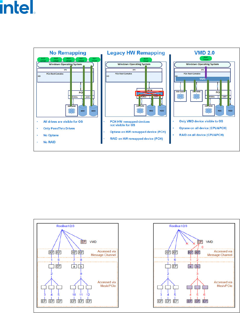
Intel Volume Management technology requires support in BIOS and driver, memory
and configuration space management.
A Volume Management Device (VMD) exposes a single device to the operating system,
which will load a single storage driver. The VMD resides in the processor's PCIe root
complex and it appears to the OS as a root bus integrated endpoint. In the processor,
the VMD is in a central location to manipulate access to storage devices which may be
attached directly to the processor or indirectly through the PCH. Instead of allowing
individual storage devices to be detected by the OS and therefore causing the OS to
load a separate driver instance for each, VMD provides configuration settings to allow
specific devices and root ports on the root bus to be invisible to the OS.
Access to these hidden target devices is provided by the VMD to the single, unified
driver.
Features Supported
Supports MMIO mapped Configuration Space (CFGBAR):
• Supports MMIO Low
R
12th Generation Intel
®
Core
™
Processors—Technologies
12
th
Generation Intel
®
Core
™
Processors
Datasheet, Volume 1 of 2 February 2023
56 Doc. No.: 655258, Rev.: 010

• Supports MMIO High
• Supports Register Lock or Restricted Access
• Supports Device Assign
• Function Assign
• MSI Remapping Disable
Deprecated Technologies
The processor has deprecated the following technologies and they are no longer
supported:
• Intel
®
Memory Protection Extensions (Intel
®
MPX)
• Branch Monitoring Counters
• Hardware Lock Elision (HLE), part of Intel
®
TSX-NI
• Intel
®
Software Guard Extensions (Intel
®
SGX)
• Intel
®
TSX-NI
• Power Aware Interrupt Routing (PAIR)
Processor Lines that support Intel's Performance Hybrid Architecture do not
support the following:
• Intel
®
Advanced Vector Extensions 512 Bit
2.9
R
Technologies—12th Generation Intel
®
Core
™
Processors
12
th
Generation Intel
®
Core
™
Processors
February 2023 Datasheet, Volume 1 of 2
Doc. No.: 655258, Rev.: 010 57
3.0 Power Management
Figure 12. Processor Power States
G0 - Working
S0 – processor Powered On
C0 – Active
P0
C1 – Auto Halt
Pn
C1E – Auto Halt – Can be in low frequency
and low voltage
C6 - All clocks are stopped, core state saved,
voltage reduced to 0v
C8 - LLC is flushed at once, display engine
still stays on
C10 – All VR’s are at PS4 or LPM + display
PSR/OFF
G1- sleeping
S3 - Hibernate – suspend to RAM (STR)
wakeup on PCH
S4 - Hibernate – suspend to Disk (STD)
wakeup on PCH
G2 - soft off
S5- power off wakeup from PCH
G3 – Mechanical off
R
12th Generation Intel
®
Core
™
Processors—Power Management
12
th
Generation Intel
®
Core
™
Processors
Datasheet, Volume 1 of 2 February 2023
58 Doc. No.: 655258, Rev.: 010
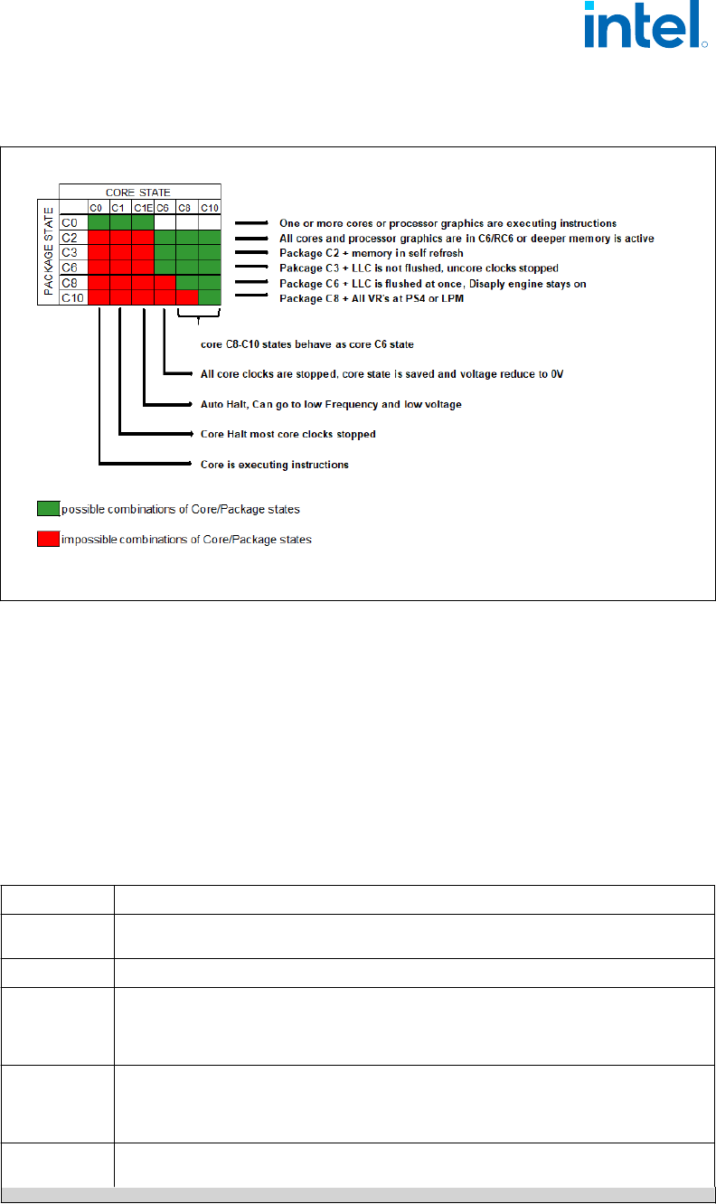
Figure 13. Processor Package and IA Core C-States
1. PkgC2/C3 are non-architectural: software cannot request to enter these states
explicitly. These states are intermediate states between PkgC0 and PkgC6.
2. There are constraints that prevent the system to go deeper.
3. The “core state” relates to the core which is in the HIGEST power state in the
package (most active).
Advanced Configuration and Power Interface (ACPI)
States Supported
This section describes the ACPI states supported by the processor.
Table 4. System States
State Description
G0/S0/C0
Full On: CPU operating. Individual devices may be shut to save power. The different CPU
operating levels are defined by Cx states.
GO/S0/Cx Cx state: CPU manages C-states by itself and can be in low power state
G1/S3
Suspend-To-RAM (STR): The system context is maintained in system DRAM, but power
is shut to non-critical circuits. Memory is retained, and refreshes continue. All external
clocks are shut off; RTC clock and internal ring oscillator clocks are still toggling.
In S3, SLP_S3 signal stays asserted, SLP_S4 and SLP_S5 are inactive until a wake occurs.
G1/S4
Suspend-To-Disk (STD): The context of the system is maintained on the disk. All power
is then shut to the system except to the logic required to resume. Externally appears same
as S5 but may have different wake events.
In S4, SLP_S3 and SLP_S4 both stay asserted and SLP_S5 is inactive until a wake occurs.
G2/S5
Soft Off: System context not maintained. All power is shut except for the logic required to
restart. A full boot is required when waking.
continued...
3.1
R
Power Management—12th Generation Intel
®
Core
™
Processors
12
th
Generation Intel
®
Core
™
Processors
February 2023 Datasheet, Volume 1 of 2
Doc. No.: 655258, Rev.: 010 59
State Description
Here, SLP_S3, SLP_S4, and SLP_S5 are all active until a wake occurs.
G3
Mechanical OFF: System context not maintained. All power shut except for the RTC. No
“Wake” events are possible because the system does not have any power. This state occurs
if the user removes the batteries, turns off a mechanical switch, or if the system power
supply is at a level that is insufficient to power the “waking” logic. When system power
returns the transition will depend on the state just prior to the entry to G3.
Table 5. Integrated Memory Controller (IMC) States
State Description
Power-Up CKE asserted. Active mode.
Pre-Charge Power Down CKE de-asserted (not self-refresh) with all banks
closed.
Active Power Down CKE de-asserted (not self-refresh) with minimum
one bank active.
Self-Refresh CKE de-asserted using device self-refresh.
Table 6. G, S, and C Interface State Combinations
Global (G)
State
Sleep (S)
State
Processor
Package (C)
State
Processor
State
System Clocks Description
G0 S0 C0 Full On On Full On
G0 S0 C2
1
Deep Sleep On Deep Sleep
G0 S0 C3
1
Deep Sleep On Deep Sleep
G0 S0 C6
Deep Power
Down
On Deep Power Down
G0 S0 C8/C10 Off On Deeper Power Down
G1 S3 Power off Off Off, except RTC Suspend to RAM
G1 S4 Power off Off Off, except RTC Suspend to Disk
G2 S5 Power off Off Off, except RTC Soft Off
G3 N/A Power off Off Power off Hard off
NOTE
1. PkgC2/C3 are non-architectural: software cannot request to enter these states
explicitly. These states are intermediate states between PkgC0 and PkgC6.
Processor IA Core Power Management
While executing code, Enhanced Intel SpeedStep
®
Technology and Intel
®
Speed Shift
technology optimizes the processor’s IA core frequency and voltage based on
workload. Each frequency and voltage operating point is defined by ACPI as a P-state.
When the processor is not executing code, it is idle. A low-power idle state is defined
by ACPI as a C-state. In general, deeper power C-states have longer entry and exit
latencies.
3.2
R
12th Generation Intel
®
Core
™
Processors—Power Management
12
th
Generation Intel
®
Core
™
Processors
Datasheet, Volume 1 of 2 February 2023
60 Doc. No.: 655258, Rev.: 010
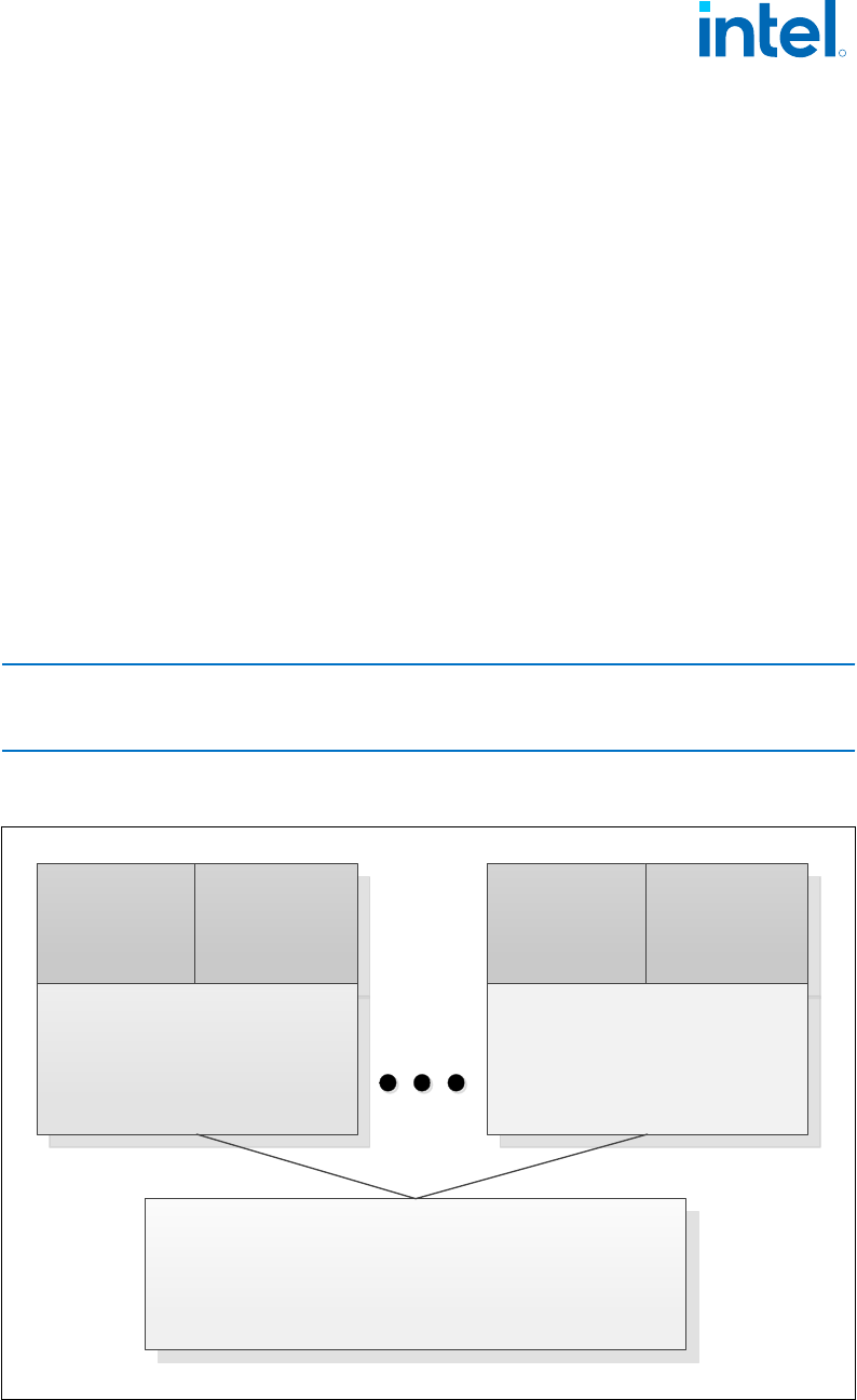
OS/HW Controlled P-states
Enhanced Intel SpeedStep
®
Technology
Enhanced Intel SpeedStep
®
Technology enables OS to control and select P-state. For
more information, refer to Enhanced Intel SpeedStep
®
Technology on page 46.
Intel
®
Speed Shift Technology
Intel
®
Speed Shift Technology is an energy efficient method of frequency control by
the hardware rather than relying on OS control. For more details, refer to Intel
®
Speed Shift Technology on page 47.
Low-Power Idle States
When the processor is idle, low-power idle states (C-states) are used to save power.
More power savings actions are taken for numerically higher C-states. However,
deeper C-states have longer exit and entry latencies. Resolution of C-states occurs at
the thread, processor IA core, and processor package level.
CAUTION
Long-term reliability cannot be assured unless all the Low-Power Idle States are
enabled.
Figure 14. Idle Power Management Breakdown of the Processor IA Cores
Thread 0 Thread 1
Core 0 State
Thread 0 Thread 1
Core N State
Processor Package State
3.2.1
3.2.1.1
3.2.1.2
3.2.2
R
Power Management—12th Generation Intel
®
Core
™
Processors
12
th
Generation Intel
®
Core
™
Processors
February 2023 Datasheet, Volume 1 of 2
Doc. No.: 655258, Rev.: 010 61

While individual threads can request low-power C-states, power saving actions only
take place once the processor IA core C-state is resolved. processor IA core C-states
are automatically resolved by the processor. For thread and processor IA core C-
states, a transition to and from C0 state is required before entering any other C-state.
Requesting the Low-Power Idle States
The primary software interfaces for requesting low-power idle states are through the
MWAIT instruction with sub-state hints and the HLT instruction (for C1 and C1E).
However, the software may make C-state requests using the legacy method of I/O
reads from the ACPI-defined processor clock control registers, referred to as P_LVLx.
This method of requesting C-states provides legacy support for operating systems that
initiate C-state transitions using I/O reads.
For legacy operating systems, P_LVLx I/O reads are converted within the processor to
the equivalent MWAIT C-state request. Therefore, P_LVLx reads do not directly result
in I/O reads to the system. The feature, known as I/O MWAIT redirection, should be
enabled in the BIOS..
The BIOS can write to the C-state range field of the PMG_IO_CAPTURE MSR to restrict
the range of I/O addresses that are trapped and emulate MWAIT like functionality. Any
P_LVLx reads outside of this range do not cause an I/O redirection to MWAIT(Cx) like
the request. They fall through like a normal I/O instruction.
When P_LVLx I/O instructions are used, MWAIT sub-states cannot be defined. The
MWAIT sub-state is always zero if I/O MWAIT redirection is used. By default, P_LVLx
I/O redirections enable the MWAIT 'break on EFLAGS.IF’ feature that triggers a wake
up on an interrupt, even if interrupts are masked by EFLAGS.IF.
Processor IA Core C-State Rules
The following are general rules for all processor IA core C-states unless specified
otherwise:
• A processor IA core C-State is determined by the lowest numerical thread state
(such as Thread 0 requests C1E while Thread 1 requests C6 state, resulting in a
processor IA core C1E state). Refer to G, S, and C Interface State Combinations
table.
• A processor IA core transitions to C0 state when:
— An interrupt occurs
— There is an access to the monitored address if the state was entered using an
MWAIT/Timed MWAIT instruction
— The deadline corresponding to the Timed MWAIT instruction expires
• An interrupt directed toward a single thread wakes up only that thread.
• If any thread in a processor IA core is active (in C0 state), the core’s C-state will
resolve to C0.
• Any interrupt coming into the processor package may wake any processor IA core.
• A system reset re-initializes all processor IA cores.
3.2.3
3.2.4
R
12th Generation Intel
®
Core
™
Processors—Power Management
12
th
Generation Intel
®
Core
™
Processors
Datasheet, Volume 1 of 2 February 2023
62 Doc. No.: 655258, Rev.: 010
Table 7. Core C-states
Core C-
State
C-State Request
Instruction
Description
C0 N/A
The normal operating state of a processor IA core where a code is being
executed
C1 MWAIT(C1)
AutoHalt - core execution stopped, autonomous clock gating (package in
C0 state)
C1E MWAIT(C1E)
Core C1 + lowest frequency and voltage operating point (package in C0
state)
C6-C10
MWAIT(C6/C8/10)
or IO
read=P_LVL3//6/8
Processor IA, flush their L1 instruction cache, the L1 data cache, and L2
cache to the LLC shared cache cores save their architectural state to an
SRAM before reducing IA cores voltage, if possible may also be reduced to
0V. Core clocks are off.
Core C-State Auto-Demotion
In general, deeper C-states, such as C6, have long latencies and have higher energy
entry/exit costs. The resulting performance and energy penalties become significant
when the entry/exit frequency of a deeper C-state is high. Therefore, incorrect or
inefficient usage of deeper C-states have a negative impact on battery life and idle
power. To increase residency and improve battery life and idle power in deeper C-
states, the processor supports C-state auto-demotion.
C-State auto-demotion:
• C6 to C1/C1E
The decision to demote a processor IA core from C6 to C1/C1E is based on each
processor IA core’s immediate residency history. Upon each processor IA core C6
request, the processor IA core C-state is demoted to C1 until a sufficient amount of
residency has been established. At that point, a processor IA core is allowed to go into
C6 . If the interrupt rate experienced on a processor IA core is high and the processor
IA core is rarely in a deep C-state between such interrupts, the processor IA core can
be demoted to a C1 state.
This feature is disabled by default. BIOS should enable it in the
PMG_CST_CONFIG_CONTROL register. The auto-demotion policy is also configured by
this register.
Package C-States
The processor supports C0, C2, C3, C6, C8, and C10 package states. The following is a
summary of the general rules for package C-state entry. These apply to all package C-
states, unless specified otherwise:
• A package C-state request is determined by the lowest numerical processor IA
core C-state amongst all processor IA cores.
• A package C-state is automatically resolved by the processor depending on the
processor IA core idle power states and the status of the platform components.
— Each processor IA core can be at a lower idle power state than the package if
the platform does not grant the processor permission to enter a requested
package C-state.
— The platform may allow additional power savings to be realized in the
processor.
3.2.5
R
Power Management—12th Generation Intel
®
Core
™
Processors
12
th
Generation Intel
®
Core
™
Processors
February 2023 Datasheet, Volume 1 of 2
Doc. No.: 655258, Rev.: 010 63
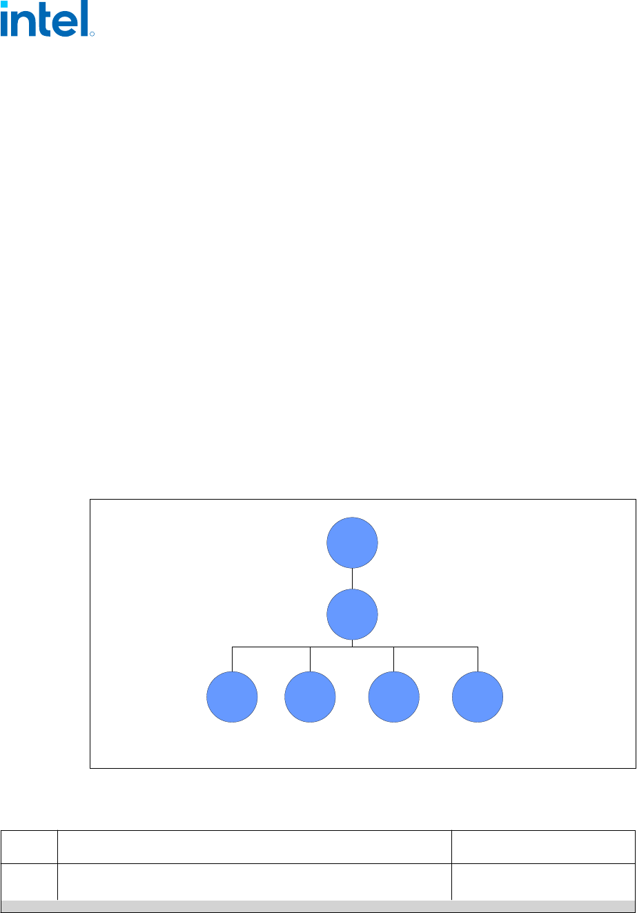
— For package C-states, the processor is not required to enter C0 before
entering any other C-state.
— Entry into a package C-state may be subject to auto-demotion – that is, the
processor may keep the package in a deeper package C-state then requested
by the operating system if the processor determines, using heuristics, that the
deeper C-state results in better power/performance.
The processor exits a package C-state when a break event is detected. Depending on
the type of break event, the processor does the following:
• If a processor IA core break event is received, the target processor IA core is
activated and the break event message is forwarded to the target processor IA
core.
— If the break event is not masked, the target processor IA core enters the
processor IA core C0 state and the processor enters package C0.
— If the break event is masked, the processor attempts to re-enter its previous
package state.
• If the break event was due to a memory access or snoop request,
— But the platform did not request to keep the processor in a higher package C-
state, the package returns to its previous C-state.
— And the platform requests a higher power C-state, the memory access or
snoop request is serviced and the package remains in the higher power C-
state.
Figure 15. Package C-State Entry and Exit
To get started, click the What is Visio? tab below
Welcome to Visio
Top tips for a simpler way to work
Package C0
Package c2
Package C6 Package C8 Package C10Package C3*
PKG C2 and C3 can not be requested explicitly by the software
Table 8. Package C-States
Package
C state
Description Dependencies
PKG C0
Processor active state.
At least one IA core in C0.
-
continued...
R
12th Generation Intel
®
Core
™
Processors—Power Management
12
th
Generation Intel
®
Core
™
Processors
Datasheet, Volume 1 of 2 February 2023
64 Doc. No.: 655258, Rev.: 010

Package
C state
Description Dependencies
Processor Graphic in RC0 (Graphics active state) or RC6 (Graphics Core power
down state).
PKG C2
Cannot be requested explicitly by the Software.
All processor IA cores in C6 or deeper + Processor Graphic cores in RC6,
memory path may be open.
The processor will enter Package C2 when:
• Transitioning from Package C0 to deep Package C state or from deep
Package C state to Package C0.
• All IA cores requested C6 or deeper + Processor Graphic cores in RC6 but
there are constraints (LTR, programmed timer events in the near future
and so forth) prevent entry to any state deeper than C2 state.
• All IA cores requested C6 or deeper + Processor Graphic cores in RC6 but
a device memory access request is received. Upon completion of all
outstanding memory requests, the processor transitions back into a
deeper package C-state.
All processor IA cores in C6 or
deeper.
Processor Graphic cores in RC6.
PKG C3
Cannot be requested explicitly by the Software.
All cores in C6 or deeper + Processor Graphics in RC6, LLC may be flushed
and turned off, memory in self refresh, memory clock stopped.
The processor will enter Package C3 when:
• All IA cores in C6 or deeper + Processor Graphic cores in RC6.
• The platform components/devices allows proper LTR for entering Package
C3.
All processor IA cores in C6 or
deeper.
Processor Graphics in RC6.
memory in self refresh, memory
clock stopped.
LLC may be flushed and turned off.
PKG C6
Package C3 + BCLK is off + IMVP9.1 VRs voltage reduction/PSx state is
possible.
The processor will enter Package C6 when:
• All IA cores in C6 or deeper + Processor Graphic cores in RC6.
• The platform components/devices allow proper LTR for entering Package
C6.
Package C3.
BCLK is off.
IMVP9.1 VRs voltage
reduction/PSx state is possible.
PKG C8
Of all IA cores requested C8 + LLC should be flushed at once, voltage will be
removed from the LLC.
The processor will enter Package C8 when:
• All IA cores in C8 or deeper + Processor Graphic cores in RC6.
• The platform components/devices allow proper LTR for entering Package
C8.
Package C6
If all IA cores requested C8, LLC is
flushed in a
single step, voltage will be
removed from the LLC.
PKG
C10
Package C8 + display in PSR or powered, all VRs at PS4 + crystal clock off.
The processor will enter Package C10 when:
• All IA cores in C10 + Processor Graphic cores in RC6.
• The platform components/devices allow proper LTR for entering Package
C10.
Package C8.
All IA cores in C8 or deeper.
Display in PSR or powered off
1
.
All VRs at PS4.
Crystal clock off.
Note: Display In PSR is only on single embedded panel configuration and panel support PSR feature.
Package C-State Auto-Demotion
The Processor may demote the Package C-State to a shallower Package C-State to
enable better performance, for example instead of going into Package C10, processor
will demote to Package C6 (and shallower as required).
The processor's decision to demote the Package C-State is based on Power
management parameters such as required C states latencies, entry/exit energy/power,
Core wake rates, and device LTR (Latency Tolerance Report). This means that the
processor is optimized to minimize platform energy for scenarios with low idle time.
R
Power Management—12th Generation Intel
®
Core
™
Processors
12
th
Generation Intel
®
Core
™
Processors
February 2023 Datasheet, Volume 1 of 2
Doc. No.: 655258, Rev.: 010 65

Processor deeper Package C-State entry frequency is controlled to minimize platform
energy. When Package C-State Auto-Demotion enabled, a reduced residency in a
deeper Package C-State is expected during system runs with high wake rates.
No change at IDLE scenario power consumption due to this feature. Package C-State
Auto-Demotion is enabled by default and controlled through BIOS menu.
Modern Standby
Modern Standby is a platform state. On display time out the OS requests the
processor to enter package C10 and platform devices at RTD3 (or disabled) in order to
attain low power in idle. Modern Standby requires proper BIOS and OS configuration.
Dynamic LLC Sizing
When all processor IA cores request C8 or deeper C-state, internal heuristics
dynamically flushes the LLC. Once the processor IA cores enter a deep C-state,
depending on their MWAIT sub-state request, the LLC is either gradually flushed N-
ways at a time or flushed all at once. Upon the processor IA cores exiting to C0 state,
the LLC is gradually expanded based on internal heuristics.
Package C-States and Display Resolutions
The integrated graphics engine has the frame buffer located in system memory. When
the display is updated, the graphics engine fetches display data from system memory.
Different screen resolutions and refresh rates have different memory latency
requirements. These requirements may limit the deepest Package C-state the
processor can enter. Other elements that may affect the deepest Package C-state
available are the following:
• Display is on or off
• Single or multiple displays
• Native or non-native resolution
• Panel Self Refresh (PSR) technology
NOTE
Display resolution is not the only factor influencing the deepest Package C-state the
processor can get into. Device latencies, interrupt response latencies, and core C-
states are among other factors that influence the final package C-state the processor
can enter.
Processor AUX Power Management
VCCIN AUX IMON Feature
This feature is the new power feature which allows the processor to read VCCIN Aux
average current via the IMVP9.1 controller over SVID.
It allows the processor to get an accurate power estimation of VCCIN Aux, which is
reflected in more accurate package power reporting and better accuracy in meeting
the package power limits (PL1, PL2, and PL3).
3.2.6
3.3
R
12th Generation Intel
®
Core
™
Processors—Power Management
12
th
Generation Intel
®
Core
™
Processors
Datasheet, Volume 1 of 2 February 2023
66 Doc. No.: 655258, Rev.: 010

VCCIN Aux IMON CPU strap will be enabled by default for best performance and
power.
Processor Graphics Power Management
Memory Power Savings Technologies
Intel
®
Rapid Memory Power Management (Intel
®
RMPM)
Intel
®
Rapid Memory Power Management (Intel
®
RMPM) conditionally places memory
into self-refresh when the processor is in package C3 or deeper power state to allow
the system to remain in the deeper power states longer for memory not reserved for
graphics memory. Intel
®
RMPM functionality depends on graphics/display state
(relevant only when processor graphics is being used), as well as memory traffic
patterns generated by other connected I/O devices.
Display Power Savings Technologies
Intel
®
Seamless Display Refresh Rate Switching Technology (Intel
®
SDRRS
Technology) with eDP* Port
Intel
®
DRRS provides a mechanism where the monitor is placed in a slower refresh
rate (the rate at which the display is updated). The system is smart enough to know
that the user is not displaying either 3D or media like a movie where specific refresh
rates are required. The technology is very useful in an environment such as a plane
where the user is in battery mode doing E-mail, or other standard office applications.
It is also useful where the user may be viewing web pages or social media sites while
in battery mode.
Intel
®
Automatic Display Brightness
Intel
®
Automatic Display Brightness feature dynamically adjusts the back-light
brightness based upon the current ambient light environment. This feature requires an
additional sensor to be on the panel front. The sensor receives the changing ambient
light conditions and sends the interrupts to the Intel Graphics driver. As per the
change in Lux, (current ambient light luminance), the new back-light setting can be
adjusted through BLC (Back Light Control). The converse applies for a brightly lit
environment. Intel
®
Automatic Display Brightness increases the back-light setting.
Smooth Brightness
The Smooth Brightness feature is the ability to make fine grained changes to the
screen brightness. All Windows* 10\11 system that support brightness control are
required to support Smooth Brightness control and it should be supporting 101 levels
of brightness control. Apart from the Graphics driver changes, there may be few
System BIOS changes required to make this feature functional.
Intel
®
Display Power Saving Technology (Intel
®
DPST) 7.0
The Intel
®
DPST technique achieves back-light power savings while maintaining a
good visual experience. This is accomplished by adaptively enhancing the displayed
image while decreasing the back-light brightness simultaneously. The goal of this
technique is to provide equivalent end-user-perceived image quality at a decreased
back-light power level.
3.4
3.4.1
3.4.2
R
Power Management—12th Generation Intel
®
Core
™
Processors
12
th
Generation Intel
®
Core
™
Processors
February 2023 Datasheet, Volume 1 of 2
Doc. No.: 655258, Rev.: 010 67

1. The original (input) image produced by the operating system or application is
analyzed by the Intel
®
DPST subsystem. An interrupt to Intel
®
DPST software is
generated whenever a meaningful change in the image attributes is detected. (A
meaningful change is when the Intel
®
DPST software algorithm determines that
enough brightness, contrast, or color change has occurred to the displaying
images that the image enhancement and back-light control needs to be altered.)
2. Intel
®
DPST subsystem applies an image-specific enhancement to increase image
contrast, brightness, and other attributes.
3. A corresponding decrease to the back-light brightness is applied simultaneously to
produce an image with similar user-perceived quality (such as brightness) as the
original image.
Intel
®
DPST 7.0 has improved power savings without adversely affecting the
performance.
Panel Self-Refresh 2 (PSR 2)
Panel Self-Refresh feature allows the Processor Graphics core to enter low-power state
when the frame buffer content is not changing constantly. This feature is available on
panels capable of supporting Panel Self-Refresh. Apart from being able to support, the
eDP* panel should be eDP 1.4 compliant. PSR 2 adds partial frame updates and
requires an eDP 1.4 compliant panel.
Low-Power Single Pipe (LPSP)
Low-power single pipe is a power conservation feature that helps save power by
keeping the inactive pipes powered OFF. This feature is enabled only in a single display
configuration without any scaling functionalities. This feature is supported from 4th
Generation Intel
®
Core
™
processor family onwards. LPSP is achieved by keeping a
single pipe enabled during eDP* only with minimal display pipeline support. This
feature is panel independent and works with any eDP panel (port A) in single display
mode.
Intel
®
Smart 2D Display Technology (Intel
®
S2DDT)
Intel
®
S2DDT reduces display refresh memory traffic by reducing memory reads
required for display refresh. Power consumption is reduced by less accesses to the
IMC. Intel S2DDT is only enabled in single pipe mode.
Intel
®
S2DDT is most effective with:
• Display images well suited to compression, such as text windows, slide shows, and
so on. Poor examples are 3D games.
• Static screens such as screens with significant portions of the background showing
2D applications, processor benchmarks, and so on, or conditions when the
processor is idle. Poor examples are full-screen 3D games and benchmarks that
flip the display image at or near display refresh rates.
Processor Graphics Core Power Savings Technologies
Intel
®
Graphics Dynamic Frequency
Intel
®
Turbo Boost Technology 2.0 is the ability of the processor IA cores and graphics
(Graphics Dynamic Frequency) cores to opportunistically increase frequency and/or
voltage above the guaranteed processor and graphics frequency for the given part.
Intel
®
Graphics Dynamic Frequency is a performance feature that makes use of
3.4.3
R
12th Generation Intel
®
Core
™
Processors—Power Management
12
th
Generation Intel
®
Core
™
Processors
Datasheet, Volume 1 of 2 February 2023
68 Doc. No.: 655258, Rev.: 010

unused package power and thermals to increase application performance. The
increase in frequency is determined by how much power and thermal budget is
available in the package, and the application demand for additional processor or
graphics performance. The processor IA core control is maintained by an embedded
controller. The graphics driver dynamically adjusts between P-States to maintain
optimal performance, power, and thermals. The graphics driver will always place the
graphics engine in its lowest possible P-State. Intel
®
Graphics Dynamic Frequency
requires BIOS support. Additional power and thermal budget should be available.
Intel
®
Graphics Render Standby Technology (Intel
®
GRST)
Intel
®
Graphics Render Standby Technology is a technique designed to optimize the
average power of the graphics part. The Graphics Render engine will be put in a sleep
state, or Render Standby (RS), during times of inactivity or basic video modes. While
in Render Standby state, the graphics part will place the VR (Voltage Regulator) into a
low voltage state. Hardware will save the render context to the allocated context
buffer when entering RS state and restore the render context upon exiting RS state.
Dynamic FPS (DFPS)
Dynamic FPS (DFPS) or dynamic frame-rate control is a runtime feature for improving
power-efficiency for 3D workloads. Its purpose is to limit the frame-rate of full screen
3D applications without compromising on user experience. By limiting the frame rate,
the load on the graphics engine is reduced, giving an opportunity to run the Processor
Graphics at lower speeds, resulting in power savings. This feature works in both
AC/DC modes.
System Agent Enhanced Intel SpeedStep
®
Technology
System Agent Enhanced Intel SpeedStep
®
Technology is a dynamic voltage frequency
scaling of the System Agent clock based on memory utilization. Unlike processor core
and package Enhanced Intel SpeedStep
®
Technology, System Agent Enhanced Intel
SpeedStep
®
Technology has three valid operating points. When running light workload
and SA Enhanced Intel SpeedStep
®
Technology is enabled, the DDR data rate may
change as follows:
BIOS/MRC DDR training at maximum, mid and minimum frequencies sets I/O and
timing parameters.
In order to achieve the optimal levels of performance and power, the memory
initialization and training process performed during first system boot or after
CMOS clear or after a BIOS update will take a longer time than a typical boot.
During this initialization and training process, end users may see a blank
screen. More information on the memory initialization process can be found
in the industry standard JEDEC Specifications found on www.JEDEC.org.
Before changing the DDR data rate, the processor sets DDR to self-refresh and
changes the needed parameters. The DDR voltage remains stable and unchanged.
Rest Of Platform (ROP) PMIC
In addition to discrete voltage regulators, Intel supports specific PMIC (Power
Management Integrated Circuit) models to power the ROP rails. PMICs are typically
classified as “Premium” or “Volume” ROP PMICs.
3.5
3.6
R
Power Management—12th Generation Intel
®
Core
™
Processors
12
th
Generation Intel
®
Core
™
Processors
February 2023 Datasheet, Volume 1 of 2
Doc. No.: 655258, Rev.: 010 69

PCI Express* Power Management
• Active power management support using L0s (see below), L1 Substates(L1.1,L1.2)
• L0s is supported on PEG10/11 interface in S/HX Processor Lines.
• L0s is supported on PEG10 interface in H Processor Lines.
• L0s is supported on PEG60 interface in H/P/U Processor Lines
• L0s is supported on PEG60/62 interface in H/P/U15 Processor Lines
• L0s is not supported on PEG60 interface in S/HX Processor Lines.
• All inputs and outputs disabled in L2/L3 Ready state.
• S Processor PCIe* interface does not support Hot-Plug.
NOTE
An increase in power consumption may be observed when PCI Express* ASPM
capabilities are disabled.
Table 9. Package C-States with PCIe* Link States Dependencies
Processor
Interface
L-State Description Package C-State
PCIe*
L1.0 or
deeper
L1- Higher latency, lower power “standby” state
L2 – Auxiliary-powered Link, deep-energy-saving
state.
Disabled - The intent of the Disabled state is to
allow a configured Link to be disabled until
directed or Electrical Idle is exited (that is, due to
a hot removal and insertion) after entering
Disabled.
No Device Attached - no physical device is
attached on PEG port
PC6-PC8
PCIe*
L1.2 or
deeper
L1- Higher latency, lower power “standby” state
L2 – Auxiliary-powered Link, deep-energy-saving
state.
Disabled - The intent of the Disabled state is to
allow a configured Link to be disabled until
directed or Electrical Idle is exited (that is, due to
a hot removal and insertion) after entering
Disabled.
No Device Attached - no physical device is
attached on PEG port
PC10
TCSS Power State
Table 10. TCSS Power State
TCSS Power
State
Allowed
Package C
Status
Device Attached Description
TC0 PC0-PC3
Yes xHCI, xDCI, USB4 controllers may be active.
USB4 DMA / PCIe may be active.
TC7 PC6-PC10
Yes xHCI and xDCI are in D3.
USB4 controller is in D3 or D0 idle.
continued...
3.7
3.8
R
12th Generation Intel
®
Core
™
Processors—Power Management
12
th
Generation Intel
®
Core
™
Processors
Datasheet, Volume 1 of 2 February 2023
70 Doc. No.: 655258, Rev.: 010
TCSS Power
State
Allowed
Package C
Status
Device Attached Description
USB4 PCIe is inactive.
TC-Cold PC3-PC10
No xHCI / xDCI / TBT DMA / TBT PCIe are in D3
IOM is active
TC10 PC6-PC10 No
Deepest Power state
xHCI and xDCI are in D3. USB4 is in D3 or D0 idle.
USB4 CIe is in inactive
IOM is inactive
IOM - TCSS Input Output Manager:
• The IOM interacts with the SoC to perform power management, boot, reset, connect and disconnect
devices to TYPE-C sub-system
TCSS Devices (xHCI / xDCI / TBT Controllers) - power states:
• D0 - Device at Active state.
• D3 - Device at lowest-powered state.
R
Power Management—12th Generation Intel
®
Core
™
Processors
12
th
Generation Intel
®
Core
™
Processors
February 2023 Datasheet, Volume 1 of 2
Doc. No.: 655258, Rev.: 010 71

4.0 Thermal Management
Processor Thermal Management
The thermal solution provides both component-level and system-level thermal
management. To allow optimal operation and long-term reliability of Intel processor-
based systems, the system/processor thermal solution should be designed so that the
processor:
• Remains below the maximum junction temperature (Tj
MAX
) specification at the
maximum Processor Base power (a.k.a TDP).
• Conforms to system constraints, such as system acoustics, system skin-
temperatures, and exhaust-temperature requirements.
CAUTION
Thermal specifications given in this chapter are on the component and package level
and apply specifically to the processor. Operating the processor outside the specified
limits may result in permanent damage to the processor and potentially other
components in the system.
Thermal Considerations
The Processor Base Power (a.k.a TDP) is the assured sustained power that should be
used for the design of the processor thermal solution, Design to a higher thermal
capability will get more Turbo residency. Processor Base Power is the time-averaged
power dissipation that the processor is validated to not exceed during manufacturing
while executing an Intel-specified high complexity workload at Base Frequency and at
the maximum junction temperature as specified in the Datasheet for the SKU segment
and configuration.
Note: The System on Chip processor integrates multiple compute cores and I/O on a
single package. Platform support for specific usage experiences may require additional
concurrency power to be considered when designing the power delivery and thermal
sustained system capability.
The processor integrates multiple processing IA cores, graphics cores and for some
SKUs a PCH on a single package. This may result in power distribution differences
across the package and should be considered when designing the thermal solution.
Intel
®
Turbo Boost Technology 2.0 allows processor IA cores to run faster than the
base frequency. It is invoked opportunistically and automatically as long as the
processor is conforming to its temperature, power, power delivery, and current control
limits. When Intel
®
Turbo Boost Technology 2.0 is enabled:
• The processor may exceed the Processor Base Power (a.k.a TDP) for short
durations to utilize any available thermal capacitance within the thermal solution.
The duration and time of such operation can be limited by platform runtime
configurable registers within the processor.
4.1
4.1.1
R
12th Generation Intel
®
Core
™
Processors—Thermal Management
12
th
Generation Intel
®
Core
™
Processors
Datasheet, Volume 1 of 2 February 2023
72 Doc. No.: 655258, Rev.: 010

• Graphics peak frequency operation is based on the assumption of only one of the
graphics domains (GT/GTx) being active. This definition is similar to the IA core
Turbo concept, where peak turbo frequency can be achieved when only one IA
core is active. Depending on the workload being applied and the distribution
across the graphics domains the user may not observe peak graphics frequency
for a given workload or benchmark.
• Thermal solutions and platform cooling that is designed to less than thermal
design guidance may experience thermal and performance issues.
NOTE
Intel
®
Turbo Boost Technology 2.0 availability may vary between the different SKUs.
Package Power Control
The package power control settings of PL1, PL2, PL3, PL4, and Tau allow the designer
to configure Intel
®
Turbo Boost Technology 2.0 to match the platform power delivery
and package thermal solution limitations.
• Power Limit 1 (PL1): A threshold for average power that will not exceed -
recommend to set to equal Processor Base Power (a.k.a TDP). PL1 should not be
set higher than thermal solution cooling limits.
• Power Limit 2 (PL2): A threshold that if exceeded, the PL2 rapid power limiting
algorithms will attempt to limit the spike above PL2.
• Power Limit 3 (PL3): A threshold that if exceeded, the PL3 rapid power limiting
algorithms will attempt to limit the duty cycle of spikes above PL3 by reactively
limiting frequency. This is an optional setting
• Power Limit 4 (PL4): A limit that will not be exceeded, the PL4 power limiting
algorithms will preemptively limit frequency to prevent spikes above PL4.
• Turbo Time Parameter (Tau): An averaging constant used for PL1 exponential
weighted moving average (EWMA) power calculation.
NOTES
1. Implementation of Intel
®
Turbo Boost Technology 2.0 only requires configuring
PL1, PL1, Tau and PL2.
2. PL3 is disabled by default.
3. The Intel Dynamic Tuning (DTT) is recommended for performance improvement in
mobile platforms. Dynamic Tuning is configured by system manufacturers
dynamically optimizing the processor power based on the current platform thermal
and power delivery conditions. Contact Intel Representatives for enabling details.
4.1.1.1
R
Thermal Management—12th Generation Intel
®
Core
™
Processors
12
th
Generation Intel
®
Core
™
Processors
February 2023 Datasheet, Volume 1 of 2
Doc. No.: 655258, Rev.: 010 73
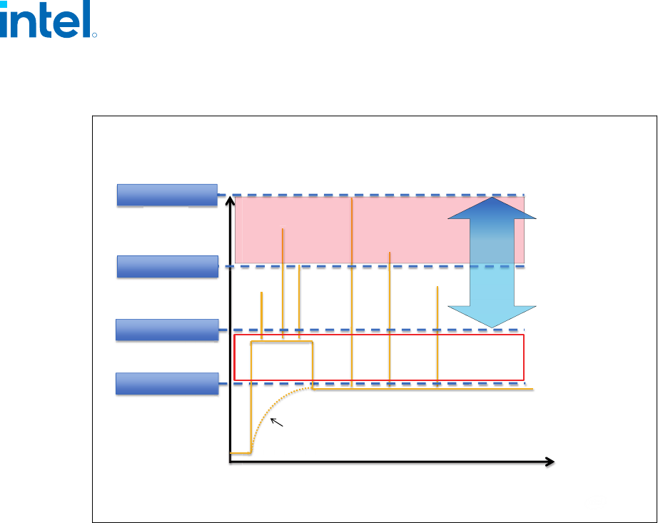
Figure 16. Package Power Control
SOC/Platform Power Limiting Knobs Options Visual
PL4
1
PL1/PsysPL1
1
PL2/PsysPL2
1
Å Power could
sustain here up to
~100s seconds
(Average power)
Time
Power
PL3
1
/PsysPL3
1
Å Power could
sustain here
forever
Note1: Optional Feature, default is disabled
Power in this region can be configured
via PL1 Tau/PsysPL1 Tau
Power
could
peak
for up
to
10ms
Duty cycles of power peaks in
this region can be configurable
via PL3/PsysPL3
Platform Power Control
The processor introduces Psys (Platform Power) to enhance processor power
management. The Psys signal needs to be sourced from a compatible charger circuit
and routed to the IMVP9 (voltage regulator). This signal will provide the total
thermally relevant platform power consumption (processor and rest of platform) via
SVID to the processor.
When the Psys signal is properly implemented, the system designer can utilize the
package power control settings of PsysPL1, PsysPL1 Tau, PsysPL2, and PsysPL3 for
additional manageability to match the platform power delivery and platform thermal
solution limitations for Intel
®
Turbo Boost Technology 2.0. The operation of the
PsysPL1, PsysPL1 Tau, PsysPL2 and PsysPL3 are analogous to the processor power
limits described in Package Power Control on page 73.
• Platform Power Limit 1 (PsysPL1): A threshold for average platform power
that will not be exceeded - recommend to set to equal platform thermal capability.
• Platform Power Limit 2 (PsysPL2): A threshold that if exceeded, the PsysPL2
rapid power limiting algorithms will attempt to limit the spikes above PsysPL2.
• Platform Power Limit 3 (PsysPL3): A threshold that if exceeded, the PsysPL3
rapid power limiting algorithms will attempt to limit the duty cycle of spikes above
PsysPL3 by reactively limiting frequency.
• PsysPL1 Tau: An averaging constant used for PsysPL1 exponential weighted
moving average (EWMA) power calculation.
4.1.1.2
R
12th Generation Intel
®
Core
™
Processors—Thermal Management
12
th
Generation Intel
®
Core
™
Processors
Datasheet, Volume 1 of 2 February 2023
74 Doc. No.: 655258, Rev.: 010

• The Psys signal and associated power limits / Tau are optional for the system
designer and disabled by default.
• The Psys data will not include power consumption for charging.
• The Intel Dynamic Tuning (DTT) is recommended for performance improvement in
mobile platforms. Dynamic Tuning is configured by system manufacturers
dynamically optimizing the processor power based on the current platform thermal
and power delivery conditions. Contact Intel Representatives for enabling details.
Turbo Time Parameter (Tau)
Turbo Time Parameter (Tau) is a mathematical parameter (units of seconds) that
controls the Intel
®
Turbo Boost Technology 2.0 algorithm. During a maximum power
turbo event, the processor could sustain PL2 for a duration longer than the Turbo Time
Parameter. If the power value and/or Turbo Time Parameter is changed during
runtime, it may take some time based on the new Turbo Time Parameter level for the
algorithm to settle at the new control limits. The time varies depending on the
magnitude of the change, power limits and other factors. There is an individual Turbo
Time Parameter associated with Package Power Control and Platform Power Control.
Assured Power (cTDP)
Assured Power (cTDP) form a design option where the processor's behavior and
package Processor Base Power (a.k.a TDP) are dynamically adjusted to a desired
system performance and power envelope. Assured Power (cTDP) technology offer
opportunities to differentiate system design while running active workloads on select
processor SKUs through scalability, configuration and adaptability. The scenarios or
methods by which each technology is used are customizable but typically involve
changes to PL1 and associated frequencies for the scenario with a resultant change in
performance depending on system's usage. Either technology can be triggered by (but
are not limited to) changes in OS power policies or hardware events such as docking a
system, flipping a switch or pressing a button. Assured Power (cTDP) is designed to be
configured dynamically and do not require an operating system reboot.
NOTE
Assured Power (cTDP) is not battery life improvement technologies.
Assured Power (cTDP)
NOTE
Assured Power) availability may vary between the different SKUs.
With Assured Power, the processor is capable of altering the maximum sustained
power with an alternate processor IA core base frequency. Assured Power allows
operation in situations where extra cooling is available or situations where a cooler
and quieter mode of operation is desired.
cTDP consists of three modes as shown in the following table.
4.1.1.3
4.1.2
4.1.2.1
R
Thermal Management—12th Generation Intel
®
Core
™
Processors
12
th
Generation Intel
®
Core
™
Processors
February 2023 Datasheet, Volume 1 of 2
Doc. No.: 655258, Rev.: 010 75

Table 11. Assured Power Modes
Mode Description
Processor Base
Power
The time-averaged power dissipation that the processor is validated to not exceed
during manufacturing while executing an Intel-specified high complexity workload at
Base Frequency and at the maximum junction temperature as specified inProcessor
Line Power and Frequency Specifications on page 85
Note: The System on Chip processor integrates multiple compute cores and I/O on a
single package. Platform support for specific usage experiences may require additional
concurrency power to be considered when designing the power delivery and thermal
sustained system capability.
Maximum Assured
Power
Maximum Assured Power ( a.k.a cTDP UP) is a specific processor IA core option, where
manufacturing confirms logical functionality within the set of operating condition limits
specified for the SKU segment.
Refer to Processor Line Power and Frequency Specifications on page 85. The Maximum
Assured Power (a.k.a cTDP-Up) Frequency and corresponding Processor Base Power is
higher than the processor IA core Base Frequency and SKU Segment Base on the
Processor Base Power.
Minimum Assured
Power
Minimum Assured Power ( a.k.a cTDP Down) is a specific processor IA core option,
where manufacturing confirms logical functionality within the set of operating condition
limits specified for the SKU segment.
Refer to Processor Line Power and Frequency Specifications on page 85. The Minimum
Assured Power ( a.k.a cTDP-Down) Frequency and corresponding Processor Base Power
(a.k.a TDP) is lower than the processor IA core Base Frequency and SKU Segment
Processor Base Power.
In each mode, the Intel
®
Turbo Boost Technology 2.0 power limits are reprogrammed
along with a new OS controlled frequency range. The Intel Dynamic Tuning driver
assists in Processor Base Power (a.k.a TDP) operation by adjusting processor PL1
dynamically. The Assured Power (cTDP) mode does not change the maximum per-
processor IA core turbo frequency.
Thermal Management Features
Occasionally the processor may operate in conditions that are near to its maximum
operating temperature. This can be due to internal overheating or overheating within
the platform. In order to protect the processor and the platform from thermal failure,
several thermal management features exist to reduce package power consumption
and thereby temperature in order to remain within normal operating limits.
Furthermore, the processor supports several methods to reduce memory power.
Adaptive Thermal Monitor
The purpose of the Adaptive Thermal Monitor is to reduce processor IA core power
consumption and temperature until it operates below its maximum operating
temperature. Processor IA core power reduction is achieved by:
• Adjusting the operating frequency (using the processor IA core ratio multiplier)
and voltage.
• Modulating (starting and stopping) the internal processor IA core clocks (duty
cycle).
The Adaptive Thermal Monitor can be activated when the package temperature,
monitored by any Digital Thermal Sensor (DTS), meets its maximum operating
temperature. The maximum operating temperature implies maximum junction
temperature Tj
MAX
.
4.1.3
4.1.3.1
R
12th Generation Intel
®
Core
™
Processors—Thermal Management
12
th
Generation Intel
®
Core
™
Processors
Datasheet, Volume 1 of 2 February 2023
76 Doc. No.: 655258, Rev.: 010

Reaching the maximum operating temperature activates the Thermal Control Circuit
(TCC). When activated the TCC causes both the processor IA core and graphics core to
reduce frequency and voltage adaptively. The Adaptive Thermal Monitor will remain
active as long as the package temperature remains at its specified limit. Therefore,
the Adaptive Thermal Monitor will continue to reduce the package frequency and
voltage until the TCC is de-activated.
Tj
MAX
is factory calibrated and is not user configurable. The default value is software
visible in the TEMPERATURE_TARGET (0x1A2) MSR, bits [23:16].
The Adaptive Thermal Monitor does not require any additional hardware, software
drivers, or interrupt handling routines. It is not intended as a mechanism to maintain
processor thermal control to PL1 = Processor Base Power. The system design should
provide a thermal solution that can maintain normal operation when PL1 = Processor
Base Power within the intended usage range.
Adaptive Thermal Monitor protection is always enabled.
TCC Activation Offset
TCC Activation Offset can be set as an offset from TjMAX to lower the onset of TCC
and Adaptive Thermal Monitor. In addition, there is an optional time window (Tau) to
manage processor performance at the TCC Activation offset value via an EWMA
(Exponential Weighted Moving Average) of temperature. For more information on TCC
Activation offset.
TCC Activation Offset with Tau=0
An offset (degrees Celsius) can be written to the TEMPERATURE_TARGET (0x1A2)
MSR, bits [29:24], the offset value will be subtracted from the value found in bits
[23:16]. When the time window (Tau) is set to zero, there will be no averaging, the
offset, will be subtracted from the TjMAX value and used as a new maximum
temperature set point for Adaptive Thermal Monitoring. This will have the same
behavior as in prior products to have TCC activation and Adaptive Thermal Monitor to
occur at this lower target silicon temperature.
If enabled, the offset should be set lower than any other passive protection such as
ACPI _PSV trip points
TCC Activation Offset with Tau
To manage the processor with the EWMA (Exponential Weighted Moving Average) of
temperature, an offset (degrees Celsius) is written to the TEMPERATURE_TARGET
(0x1A2) MSR, bits [29:24], and the time window (Tau) is written to the
TEMPERATURE_TARGET (0x1A2) MSR [6:0]. The Offset value will be subtracted from
the value found in bits [23:16] and be the temperature.
The processor will manage to this average temperature by adjusting the frequency of
the various domains. The instantaneous Tj can briefly exceed the average
temperature. The magnitude and duration of the overshoot is managed by the time
window value (Tau).
This averaged temperature thermal management mechanism is in addition, and not
instead of TjMAX thermal management. That is, whether the TCC activation offset is 0
or not, TCC Activation will occur at TjMAX.
Frequency / Voltage Control
R
Thermal Management—12th Generation Intel
®
Core
™
Processors
12
th
Generation Intel
®
Core
™
Processors
February 2023 Datasheet, Volume 1 of 2
Doc. No.: 655258, Rev.: 010 77

Upon Adaptive Thermal Monitor activation, the processor attempts to dynamically
reduce processor temperature by lowering the frequency and voltage operating point.
The operating points are automatically calculated by the processor IA core itself and
do not require the BIOS to program them as with previous generations of Intel
processors. The processor IA core will scale the operating points such that:
• The voltage will be optimized according to the temperature, the processor IA core
bus ratio and the number of processor IA cores in deep C-states.
• The processor IA core power and temperature are reduced while minimizing
performance degradation.
Once the temperature has dropped below the trigger temperature, the operating
frequency and voltage will transition back to the normal system operating point.
Once a target frequency/bus ratio is resolved, the processor IA core will transition to
the new target automatically.
• On an upward operating point transition, the voltage transition precedes the
frequency transition.
• On a downward transition, the frequency transition precedes the voltage
transition.
• The processor continues to execute instructions. However, the processor will halt
instruction execution for frequency transitions.
If a processor load-based Enhanced Intel SpeedStep Technology/P-state transition
(through MSR write) is initiated while the Adaptive Thermal Monitor is active, there
are two possible outcomes:
• If the P-state target frequency is higher than the processor IA core optimized
target frequency, the P-state transition will be deferred until the thermal event has
been completed.
• If the P-state target frequency is lower than the processor IA core optimized
target frequency, the processor will transition to the P-state operating point.
Clock Modulation
If the frequency/voltage changes are unable to end an Adaptive Thermal Monitor
event, the Adaptive Thermal Monitor will utilize clock modulation. Clock modulation is
done by alternately turning the clocks off and on at a duty cycle (ratio between clock
“on” time and total time) specific to the processor. The duty cycle is factory configured
to 25% on and 75% off and cannot be modified. The period of the duty cycle is
configured to 32 microseconds when the Adaptive Thermal Monitor is active. Cycle
times are independent of processor frequency. A small amount of hysteresis has been
included to prevent excessive clock modulation when the processor temperature is
near its maximum operating temperature. Once the temperature has dropped below
the maximum operating temperature, and the hysteresis timer has expired, the
Adaptive Thermal Monitor goes inactive and clock modulation ceases. Clock
modulation is automatically engaged as part of the Adaptive Thermal Monitor
activation when the frequency/voltage targets are at their minimum settings.
Processor performance will be decreased when clock modulation is active. Snooping
and interrupt processing are performed in the normal manner while the Adaptive
Thermal Monitor is active.
Clock modulation will not be activated by the Package average temperature control
mechanism.
R
12th Generation Intel
®
Core
™
Processors—Thermal Management
12
th
Generation Intel
®
Core
™
Processors
Datasheet, Volume 1 of 2 February 2023
78 Doc. No.: 655258, Rev.: 010

Thermal Throttling
As the processor approaches TJMax a throttling mechanisms will engage to protect the
processor from over-heating and provide control thermal budgets.
Achieving this is done by reducing IA and other subsystem agent's voltages and
frequencies in a gradual and coordinated manner that varies depending on the
dynamics of the situation. IA frequencies and voltages will be directed down as low as
LFM (Lowest Frequency Mode). In relatively rare cases, the processor may take
throttle actions on the IO domain, which includes IO fabrics and device throttling, that
are designed to avoid shutdown of the system. Further restricts are possible via
Thermal Trolling point (TT1) under conditions where thermal budget cannot be re-
gained fast enough with voltages and frequencies reduction alone. TT1 keeps the
same processor voltage and clock frequencies the same yet skips clock edges to
produce effectively slower clocking rates. This will effectively result in observed
frequencies below LFM on the Windows PERF monitor.
Digital Thermal Sensor
Each processor has multiple on-die Digital Thermal Sensor (DTS) that detects the
processor IA, GT and other areas of interest instantaneous temperature.
Temperature values from the DTS can be retrieved through:
• A software interface using processor Model Specific Register (MSR).
• A processor hardware interface.
When the temperature is retrieved by the processor MSR, it is the instantaneous
temperature of the given DTS. When the temperature is retrieved using PECI, it is the
average of the highest DTS temperature in the package over a 256 ms time window.
Intel recommends using the PECI reported temperature for platform thermal control
that benefits from averaging, such as fan speed control. The average DTS temperature
may not be a good indicator of package Adaptive Thermal Monitor activation or rapid
increases in temperature that triggers the Out of Specification status bit within the
PACKAGE_THERM_STATUS (0x1B1) MSR and IA32_THERM_STATUS (0x19C) MSR.
Code execution is halted in C1 or deeper C-states. Package temperature can still be
monitored through PECI in lower C-states.
Unlike traditional thermal devices, the DTS outputs a temperature relative to the
maximum supported operating temperature of the processor (Tj
MAX
), regardless of
TCC activation offset. It is the responsibility of software to convert the relative
temperature to an absolute temperature. The absolute reference temperature is
readable in the TEMPERATURE_TARGET (0x1A2) MSR. The temperature returned by
the DTS is an implied negative integer indicating the relative offset from Tj
MAX
. The
DTS does not report temperatures greater than Tj
MAX
. The DTS-relative temperature
readout directly impacts the Adaptive Thermal Monitor trigger point. When a package
DTS indicates that it has reached the TCC activation (a reading of 0x0, except when
the TCC activation offset is changed), the TCC will activate and indicate an Adaptive
Thermal Monitor event. A TCC activation will lower both processor IA core and
graphics core frequency, voltage, or both. Changes to the temperature can be
detected using two programmable thresholds located in the processor thermal MSRs.
These thresholds have the capability of generating interrupts using the processor IA
core's local APIC. Refer to the Intel 64 Architectures Software Developer’s Manual for
specific register and programming details.
Digital Thermal Sensor Accuracy (T_accuracy)
4.1.3.2
R
Thermal Management—12th Generation Intel
®
Core
™
Processors
12
th
Generation Intel
®
Core
™
Processors
February 2023 Datasheet, Volume 1 of 2
Doc. No.: 655258, Rev.: 010 79

The error associated with DTS measurements will not exceed ±5 °C within the entire
operating range.
Fan Speed Control with Digital Thermal Sensor
Digital Thermal Sensor based fan speed control (T
FAN
) is a recommended feature to
achieve optimal thermal performance. At the T
FAN
temperature, Intel recommends full
cooling capability before the DTS reading reaches Tj
MAX
.
PROCHOT# Signal
The PROCHOT# (processor hot) signal is asserted by the processor when the TCC is
active. Only a single PROCHOT# pin exists at a package level. When any DTS
temperature reaches the TCC activation temperature, the PROCHOT# signal will be
asserted. PROCHOT# assertion policies are independent of Adaptive Thermal Monitor
enabling.
The PROCHOT# signal can be configured to the following modes:
• Input Only: PROCHOT is driven by an external device.
• Output Only: PROCHOT is driven by processor.
• Bi-Directional: Both Processor and external device can drive PROCHOT signal
PROCHOT Input Only
The PROCHOT# signal should be set to input only by default. In this state, the
processor will only monitor PROCHOT# assertions and respond by setting the
maximum frequency to 10Khz.
The following two features are enabled when PROCHOT is set to Input only:
• Fast PROCHOT: Respond to PROCHOT# within 1uS of PROCHOT# pin assertion,
reducing the processor power.
• PROCHOT Demotion Algorithm: designed to improve system performance
during multiple PROCHOT assertions.
PROCHOT Output Only
Legacy state, PROCHOT is driven by the processor to external device.
Bi-Directional PROCHOT#
By default, the PROCHOT# signal is set to input only. When configured as an input or
bi-directional signal, PROCHOT# can be used for thermally protecting other platform
components should they overheat as well. When PROCHOT# is driven by an external
device:
• The package will immediately transition to the lowest P-State (Pn) supported by
the processor IA cores and graphics cores. This is contrary to the internally-
generated Adaptive Thermal Monitor response.
• Clock modulation is not activated.
The processor package will remain at the lowest supported P-state until the system
de-asserts PROCHOT#. The processor can be configured to generate an interrupt upon
assertion and de-assertion of the PROCHOT# signal.
4.1.3.3
4.1.3.4
4.1.3.5
R
12th Generation Intel
®
Core
™
Processors—Thermal Management
12
th
Generation Intel
®
Core
™
Processors
Datasheet, Volume 1 of 2 February 2023
80 Doc. No.: 655258, Rev.: 010
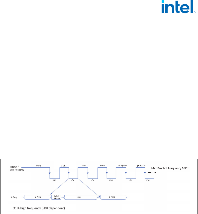
When PROCHOT# is configured as a bi-directional signal and PROCHOT# is asserted
by the processor, it is impossible for the processor to detect a system assertion of
PROCHOT#. The system assertion will have to wait until the processor de-asserts
PROCHOT# before PROCHOT# action can occur due to the system assertion. While the
processor is hot and asserting PROCHOT#, the power is reduced but the reduction rate
is slower than the system PROCHOT# response of < 100 us. The processor thermal
control is staged in smaller increments over many milliseconds. This may cause
several milliseconds of delay to a system assertion of PROCHOT# while the output
function is asserted.
PROCHOT Demotion Algorithm
PROCHOT demotion algorithm is designed to improve system performance following
multiple Platform PROCHOT consecutive assertions. During each PROCHOT assertion
processor will eventually transition to the lowest P-State (Pn) supported by the
processor IA cores and graphics cores (LFM). When detecting several PROCHOT
consecutive assertions the processor will reduce the max frequency in order to reduce
the PROCHOT assertions events. The processor will keep reducing the frequency until
no consecutive assertions detected. The processor will raise the frequency if no
consecutive PROCHOT assertion events will occur. PROCHOT demotion algorithm
enabled only when the PROCHOT is configured as input.
Figure 17. PROCHOT Demotion Signal Description
Voltage Regulator Protection using PROCHOT#
PROCHOT# may be used for thermal protection of voltage regulators (VR). System
designers can create a circuit to monitor the VR temperature and assert PROCHOT#
and, if enabled, activate the TCC when the temperature limit of the VR is reached.
When PROCHOT# is configured as a bi-directional or input only signal, if the system
assertion of PROCHOT# is recognized by the processor, results in power reduction.
Power reduction down to LFM and duration of the platform PROCHOT# assertion
supported by the processor IA cores and graphics cores. Systems should still provide
proper cooling for the VR and rely on bi-directional PROCHOT# only as a backup in
case of system cooling failure. Overall, the system thermal design should allow the
power delivery circuitry to operate within its temperature specification even while the
processor is operating at its Processor Base Power.
Thermal Solution Design and PROCHOT# Behavior
With a properly designed and characterized thermal solution, it is anticipated that
PROCHOT# will only be asserted for very short periods of time when running the most
power intensive applications. The processor performance impact due to these brief
4.1.3.6
4.1.3.7
4.1.3.8
R
Thermal Management—12th Generation Intel
®
Core
™
Processors
12
th
Generation Intel
®
Core
™
Processors
February 2023 Datasheet, Volume 1 of 2
Doc. No.: 655258, Rev.: 010 81

periods of TCC activation is expected to be so minor that it would be immeasurable.
However, an under-designed thermal solution that is not able to prevent excessive
assertion of PROCHOT# in the anticipated ambient environment may:
• Cause a noticeable performance loss.
• Result in prolonged operation at or above the specified maximum junction
temperature and affect the long-term reliability of the processor.
• May be incapable of cooling the processor even when the TCC is active
continuously (in extreme situations).
Low-Power States and PROCHOT# Behavior
Depending on package power levels during package C-states, outbound PROCHOT#
may de-assert while the processor is idle as power is removed from the signal. Upon
wake up, if the processor is still hot, the PROCHOT# will re-assert, although typically
package idle state residency should resolve any thermal issues. The PECI interface is
fully operational during all C-states and it is expected that the platform continues to
manage processor IA core and package thermals even during idle states by regularly
polling for thermal data over PECI.
THRMTRIP# Signal
Regardless of enabling the automatic or on-demand modes, in the event of a
catastrophic cooling failure, the package will automatically shut down when the silicon
has reached an elevated temperature that risks physical damage to the product. At
this point, the THRMTRIP# signal will go active.
Critical Temperature Detection
Critical Temperature detection is performed by monitoring the package temperature.
This feature is intended for graceful shutdown before the THRMTRIP# is activated.
However, the processor execution is not guaranteed between critical temperature and
THRMTRIP#. If the Adaptive Thermal Monitor is triggered and the temperature
remains high, a critical temperature status and sticky bit are latched in the
PACKAGE_THERM_STATUS (0x1B1) MSR and the condition also generates a thermal
interrupt, if enabled.
On-Demand Mode
The processor provides an auxiliary mechanism that allows system software to force
the processor to reduce its power consumption using clock modulation. This
mechanism is referred to as “On-Demand” mode and is distinct from Adaptive Thermal
Monitor and bi-directional PROCHOT#. The processor platforms should not rely on
software usage of this mechanism to limit the processor temperature. On-Demand
Mode can be accomplished using processor MSR or chipset I/O emulation. On-Demand
Mode may be used in conjunction with the Adaptive Thermal Monitor. However, if the
system software tries to enable On-Demand mode at the same time the TCC is
engaged, the factory configured the duty cycle of the TCC will override the duty cycle
selected by the On-Demand mode. If the I/O based and MSR-based On-Demand
modes are in conflict, the duty cycle selected by the I/O emulation-based On-Demand
mode will take precedence over the MSR-based On-Demand Mode.
4.1.3.9
4.1.3.10
4.1.3.11
4.1.3.12
R
12th Generation Intel
®
Core
™
Processors—Thermal Management
12
th
Generation Intel
®
Core
™
Processors
Datasheet, Volume 1 of 2 February 2023
82 Doc. No.: 655258, Rev.: 010

MSR Based On-Demand Mode
If Bit 4 of the IA32_CLOCK_MODULATION MSR is set to 1, the processor will
immediately reduce its power consumption using modulation of the internal processor
IA core clock, independent of the processor temperature. The duty cycle of the clock
modulation is programmable using bits [3:1] of the same IA32_CLOCK_MODULATION
MSR. In this mode, the duty cycle can be programmed in either 12.5% or 6.25%
increments (discoverable using CPUID). Thermal throttling using this method will
modulate each processor IA core's clock independently.
I/O Emulation-Based On-Demand Mode
I/O emulation-based clock modulation provides legacy support for operating system
software that initiates clock modulation through I/O writes to ACPI defined processor
clock control registers on the chipset (PROC_CNT). Thermal throttling using this
method will modulate all processor IA cores simultaneously.
Intel
®
Memory Thermal Management
DRAM Thermal Aggregation
P-Unit firmware is responsible for aggregating DRAM temperature sources into a per-
DIMM reading as well as an aggregated virtual 'max' sensor reading. At reset, MRC
communicates to the MC the valid channels and ranks as well as DRAM type. At that
time, Punit firmware sets up a valid channel and rank mask that is then used in the
thermal aggregation algorithm to produce a single maximum temperature
DRAM Thermal Monitoring
• DRAM thermal sensing Periodic DDR thermal reads from DDR
• DRAM thermal calculation Punit reads of DDR thermal information direct from the
memory controller (MR4 or MPR) Punit estimation of a virtual maximum DRAM
temperature based on per-rank readings. Application of thermal filter to the virtual
maximum temperature.
DRAM Refresh Rate Control
The MRC will natively interface with MR4 or MPR readings to adjust DRAM refresh rate
as needed to maintain data integrity. This capability is enabled by default and occurs
automatically. Direct override of this capability is available for debug purposes, but
this cannot be adjusted during runtime.
Processor Line Thermal and Power Specifications
The following notes apply to Processor Line Power and Frequency Specifications on
page 85, Table 19 on page 92, Table 17 on page 89
4.1.3.13
4.1.3.14
4.1.4
4.2
R
Thermal Management—12th Generation Intel
®
Core
™
Processors
12
th
Generation Intel
®
Core
™
Processors
February 2023 Datasheet, Volume 1 of 2
Doc. No.: 655258, Rev.: 010 83

Note Definition
1
The Processor Base Power (a.k.a TDP) and Assured Power (cTDP) values are the average power
dissipation in junction temperature operating condition limit, for the SKU Segment and
Configuration, for which the processor is validated during manufacturing when executing an
associated Intel-specified high-complexity workload at the processor IA core frequency
corresponding to the configuration and SKU.
2
Thermal workload (Processor Base Power (a.k.a TDP)) may consist of a combination of processor IA
core intensive and graphics core intensive applications.
3 Can be modified at runtime by MSR writes, with MMIO and with PECI commands.
4
'Turbo Time Parameter' is a mathematical parameter (units of seconds) that controls the processor
turbo algorithm using a moving average of energy usage. Do not set the Turbo Time Parameter to a
value less than 0.1 seconds. refer to Platform Power Control on page 74 for further information.
5
The shown limit is a time averaged-power, based upon the Turbo Time Parameter. Absolute product
power may exceed the set limits for short durations or under virus or uncharacterized workloads.
6
The Processor will be controlled to a specified power limit as described in Intel
®
Turbo Boost
Technology 2.0 Power Monitoring on page 45. If the power value and/or 'Turbo Time Parameter' is
changed during runtime, it may take a short period of time (approximately 3 to 5 times the 'Turbo
Time Parameter') for the algorithm to settle at the new control limits.
7 This is a hardware default setting and not a behavioral characteristic of the part.
8 For controllable turbo workloads, the PL2 limit may be exceeded for up to 10ms.
9
LPM power level is an opportunistic power and is not a guaranteed value as usages and
implementations may vary.
10
Power limits may vary depending on if the product supports the Minimum Assured Power (cTDP
Down) and/or Maximum Assured Power (cTDP Up) modes. Default power limits can be found in the
PKG_PWR_SKU MSR (614h).
11
The processor die do not reach maximum sustained power simultaneously since the sum of the 2
die's estimated power budget is controlled to be equal to or less than the package Processor Base
Power (a.k.a TDP) (PL1) limit.
12
Minimum Assured Power(cTDP Down) power is based on 96EU equivalent graphics configuration.
Minimum Assured Power(cTDP Down) does not decrease the number of active Processor Graphics
EUs but relies on Power Budget Management (PL1) to achieve the specified power level.
13 May vary based on SKU.
14
• The formula of PL2=PL1*1.25 is the hardware.
• PL2- SoC opportunistic higher Average Power with limited duration controlled by Tau_PL1
setting, the larger the Tau, the longer the PL2 duration.
• A recommendation to set all power delivery especially PL2 and PL1 based on platform power and
thermal capability via BIOS.
15
Possessor Base Power (a.k.a TDP) workload does not reflect various I/O connectivity cases such as
Thunderbolt.
16
Hardware default of PL1 Tau=1s, By including the benefits available from power and thermal
management features the recommended is to use PL1 Tau=28s.
R
12th Generation Intel
®
Core
™
Processors—Thermal Management
12
th
Generation Intel
®
Core
™
Processors
Datasheet, Volume 1 of 2 February 2023
84 Doc. No.: 655258, Rev.: 010
Processor Line Power and Frequency Specifications
Table 12. Processor Base Power (TDP) and Frequency Specifications(H-Processor Line,
P-Processor Line)
Segment
and
Package
Processor
IA/GT Cores,
and Processor
Base Power
Configuration
Processor IA
Core Frequency
Graphics Core
Frequency
Processor Base
Power [w]
Notes
H-
Processor
Line
BGA
6+8 Core 45W
Maximum Assured
Power
2.7GHz up to
2.9GHz
300MHz
65
1,9,10,
11,12,
15
P-Core
2.3GHz up to
2.5GHz
45
E-Core
1.7GHz up to
1.8GHz
Minimum Assured
Power
1.5GHz up to
1.9GHz
35
LFM 400MHZ 100MHz N/A
H-
Processor
Line
BGA
6+4 Core 45W
Maximum Assured
Power
2.7GHz
300MHz
65
P-Core 2.3GHz
45
1,9,10,
11,12,
15
E-Core 1.7GHz
Minimum Assured
Power
1.5GHz 35
LFM 400MHZ 100MHz N/A
H-
Processor
Line
BGA
4+8 Core 45W
Maximum Assured
Power
3.1GHz up to
3.2GHz
300MHz
65
P-Core
2.5GHz up to
2.7GHz
45
1,9,10,
11,12,
15
E-Core
1.8GHz up to
2.0GHz
Minimum Assured
Power
1.7GHz up to
2.2GHz
35
LFM 400MHZ 100MHz N/A
H-
Processor
Line
BGA
4+4 Core 45W
Maximum Assured
Power
2.5GHz
300MHz
65
P-Core 2.0GHz
45
E-Core 1.5GHz
Minimum Assured
Power
1.1GHz 35
LFM 400MHZ 100MHz N/A
P-Processor
Line BGA
6+8 Core 28W
Maximum Assured
Power
2GHz
300MHz
35
1,9,10,
11,12,
15
P-Core 1.8GHz
28
E-Core 1.3GHz
Minimum Assured
Power
1.4GHz 20
continued...
4.2.1
R
Thermal Management—12th Generation Intel
®
Core
™
Processors
12
th
Generation Intel
®
Core
™
Processors
February 2023 Datasheet, Volume 1 of 2
Doc. No.: 655258, Rev.: 010 85
Segment
and
Package
Processor
IA/GT Cores,
and Processor
Base Power
Configuration
Processor IA
Core Frequency
Graphics Core
Frequency
Processor Base
Power [w]
Notes
LFM 400MHZ 100MHz N/A
P-Processor
Line BGA
4+8 Core 28W
Maximum Assured
Power
2.1GHz up to
2.5GHz
300MHz
35
1,9,10,
11,12,
15
P-Core
1.7GHz up to
2.2GHz
28
E-Core
1.2GHz up to
1.6GHz
Minimum Assured
Power
1.4GHz up to
1.6GHz
20
LFM 400MHZ 100MHz N/A
P-Processor
Line BGA
2+8 Core 28W
Maximum Assured
Power
2GHz
300MHz
35
1,9,10,
11,12,
15
P-Core 1.5GHz
28
E-Core 1.1Ghz
Minimum Assured
Power
1.0GHz 20
LFM 400MHZ 100MHz N/A
Table 13. Processor Base Power (TDP) and Frequency Specifications(U-Processor Line)
Segment
and
Package
Processor
IA/GT Cores,
and Processor
Base Power
Configuration
Processor IA
Core Frequency
Graphics Core
Frequency
Processor Base
Power [w]
Notes
U-
Processor
Line BGA
2+8 Core 15W
Maximum Assured
Power
2.5GHz up to
2.7GHz
300MHz
28
1,9,10,
11,12,
15
P-Core
1.3GHz up to
1.8GHz
15
E-Core
0.9GHz up to
1.3GHz
Minimum Assured
Power
0.8GHz up to
1.3GHz
12
LFM 400MHZ 100MHz N/A
U-
Processor
Line BGA
2+4 Core 15W
Maximum Assured
Power
2.5GHz
300MHz
28
1,9,10,
11,12,
15
P-Core 1.2GHz
15
E-Core 0.9GHz
Minimum Assured
Power
0.8GHz 12
LFM 400MHZ 100MHz N/A
U-
Processor
Line BGA
1+4 Core 15W
Maximum Assured
Power
2.5GHz
300MHz
28
1,9,10,
11,12,
15
P-Core
1.1GHz up to
1.2GHz
15
continued...
R
12th Generation Intel
®
Core
™
Processors—Thermal Management
12
th
Generation Intel
®
Core
™
Processors
Datasheet, Volume 1 of 2 February 2023
86 Doc. No.: 655258, Rev.: 010
Segment
and
Package
Processor
IA/GT Cores,
and Processor
Base Power
Configuration
Processor IA
Core Frequency
Graphics Core
Frequency
Processor Base
Power [w]
Notes
E-Core 0.9GHz
Minimum Assured
Power
0.8GHz up to
0.9GHz
12
LFM 400MHZ 100MHz N/A
Table 14. Processor Base Power (TDP) and Frequency Specifications (U 9W-Processor
Line)
Segment
and
Package
Processor
IA /GT Cores,
and Processor
Base Power
Configuration
Processor IA
Core Frequency
Graphics Core
Frequency
Processor Base
Power [w]
Notes
U-
Processor
Line BGA
2+8 Core 9W
Maximum Assured
Power
1.7GHz up to
1.9GHz
300MHz
15
1,9,10,
11,12,
15
P-Core
1.0GHz up to
1.1GHz
9
E-Core
0.7GHz up to
0.8GHz
LFM 400MHZ 100MHz N/A
U-
Processor
Line BGA
2+4 Core 9W
Maximum Assured
Power
1.7GHz
300MHz
15
1,9,10,
11,12,
15
P-Core 1.0GHz
9
E-Core 0.7GHz
LFM 400MHZ 100MHz N/A
U-
Processor
Line BGA
1+4 Core 9W
Maximum Assured
Power
1.6GHz
300MHz
15
1,9,10,
11,12,
15
P-Core 1.0GHz
9
E-Core 0.7GHz
LFM 400MHZ 100MHz N/A
Table 15. Processor Base Power (TDP) and Frequency Specifications (S-Processor Line)
Segment and
Package
Processor
IA/GT Cores,
and Processor
Base Power
Configuration
Processor IA
Core Frequency
Graphics Core
Frequency
Processor
Base Power
[w]
Notes
S-Processor Line
LGA
8+8 Core 150W
P-Core 3.4 GHz
300MHZ 150
1,9,10,
11,12,
15
E-Core 2.5 GHz
LFM 400MHZ 300MHZ N/A
S-Processor Line
LGA
8+8 Core 125W
P-Core 3.2GHz
300MHZ 125
1,9,10,
11,12,
15
E-Core 2.4GHz
LFM 400MHZ 300MHZ N/A
continued...
R
Thermal Management—12th Generation Intel
®
Core
™
Processors
12
th
Generation Intel
®
Core
™
Processors
February 2023 Datasheet, Volume 1 of 2
Doc. No.: 655258, Rev.: 010 87
Segment and
Package
Processor
IA/GT Cores,
and Processor
Base Power
Configuration
Processor IA
Core Frequency
Graphics Core
Frequency
Processor
Base Power
[w]
Notes
S-Processor Line
LGA
8+4 Core 125W
P-Core 3.6GHz
300MHZ 125
1,9,10,
11,12,
15
E-Core 2.7GHz
LFM 400MHZ 300MHZ N/A
S-Processor Line
LGA
6+4 Core 125W
P-Core 3.7GHz
300MHZ 125
1,9,10,
11,12,
15
E-Core 2.8GHz
LFM 400MHZ 300MHZ N/A
S-Processor Line
LGA
8+8 Core 65W
P-Core 2.4GHz
300MHZ
65
1,9,10,
11,12,
15
E-Core 1.8GHz
LFM 400MHZ N/A
S-Processor Line
LGA
8+4 Core 65W
P-Core 2.1GHz
300MHZ
65
1,9,10,
11,12,
15
E-Core 1.6GHz
LFM 400MHZ N/A
S-Processor Line
LGA
8+8 Core 35W
P-Core 1.4GHz
300MHZ
35
1,9,10,
11,12,
15
E-Core 1GHz
LFM 400MHZ N/A
S-Processor Line
LGA
8+4 Core 35W
P-Core 1.4GHz
300MHZ
35
1,9,10,
11,12,
15
E-Core 1GHz
LFM 400MHZ N/A
S-Processor Line
LGA
6+0 Core 35W
P-Core
1.8GHz up to
2.1GHz
300MHZ
35
1,9,10,
11,12,
15
LFM 1GHz N/A
S-Processor Line
LGA
4+0 Core 35W
P-Core
2.2GHz up to
2.3GHz
300MHZ
35
1,9,10,
11,12,
15
LFM 400MHZ N/A
S-Processor Line
LGA
2+0 Core 35W
P-Core
2.8GHz up to
3.1GHz
300MHZ
35
1,9,10,
11,12,
15
LFM 400MHZ N/A
S-Processor Line
LGA
6+0 Core 65W
P-Core
2.5GHz up to
3.3GHz
300MHZ
65
1,9,10,
11,12,
15
LFM 400MHZ N/A
S-Processor Line
LGA
4+0 Core 60W
P-Core
3.3GHz up to
3.5GHz
300MHZ
60
1,9,10,
11,12,
15
LFM 400MHZ N/A
S-Processor Line
LGA
4+0 Core 58W
P-Core 3.3GHz
300MHZ
58
1,9,10,
11,12,
15
continued...
R
12th Generation Intel
®
Core
™
Processors—Thermal Management
12
th
Generation Intel
®
Core
™
Processors
Datasheet, Volume 1 of 2 February 2023
88 Doc. No.: 655258, Rev.: 010
Segment and
Package
Processor
IA/GT Cores,
and Processor
Base Power
Configuration
Processor IA
Core Frequency
Graphics Core
Frequency
Processor
Base Power
[w]
Notes
LFM 400MHZ N/A
S-Processor Line
LGA
2+0 Core 46W
P-Core
3.4GHz up to
3.7GHz
300MHZ
46
1,9,10,
11,12,
15
LFM 400MHZ N/A
Table 16. Processor Base Power (TDP) and Frequency Specifications (HX-Processor
Line)
Segment
and
Package
Processor
IA/GT Cores,
and Processor
Base Power
Configuration
Processor IA
Core Frequency
Graphics Core
Frequency
Processor Base
Power [w]
Notes
HX-
Processor
Line SBGA
8+8 Core 55W
P-Core
2 GHz up to 2.3
GHz
300 MHZ
55 W
1,9,10,
11,12,
15
E-Core
1.5 GHz up to 1.7
GHz
45 W
Minimum Assured
Power
(Configurable
TDP-Down )
1.7 GHz up to 2
GHz
LFM 0.8 GHz N/A
HX-
Processor
Line SBGA
4+8 Core 55W
P-Core 2.5 GHz
300 MHZ
55 W
E-Core 1.8 GHz
45 W
Minimum Assured
Power
(Configurable
TDP-Down )
2.1 GHz
LFM 0.8 GHz N/A
Processor Line Thermal and Power
Table 17. Package Turbo Specifications (H/P/U -Processor Lines)
Segment and
Package
Processor IA
Cores,
Graphics,
Configuration
and Processor
Base Power
(a.k.a. TDP)
Parameter Minimum
Recommended
Value
Tau MSR
Max
Value
Units Notes
H-Processor
Line
6+8 Core 45W
Power Limit 1
Time (PL1 Tau)
0.1 56 448 S
3,4,5,6,
7,8,14,1
6,17
Power Limit 1
(PL1)
N/A 45 N/A W
Power Limit 2
(PL2)
N/A 115 N/A W
H-Processor
Line
6+4 Core 45W
Power Limit 1
Time (PL1 Tau)
0.1 56 448 S
3,4,5,6,
7,8,14,1
6,17
continued...
4.2.2
R
Thermal Management—12th Generation Intel
®
Core
™
Processors
12
th
Generation Intel
®
Core
™
Processors
February 2023 Datasheet, Volume 1 of 2
Doc. No.: 655258, Rev.: 010 89
Segment and
Package
Processor IA
Cores,
Graphics,
Configuration
and Processor
Base Power
(a.k.a. TDP)
Parameter Minimum
Recommended
Value
Tau MSR
Max
Value
Units Notes
Power Limit 1
(PL1)
N/A 45 N/A W
Power Limit 2
(PL2)
N/A 115 N/A W
H-Processor
Line
4+8 Core 45W
Power Limit 1
Time (PL1 Tau)
0.1 56 448 S
3,4,5,6,
7,8,14,1
6,17
Power Limit 1
(PL1)
N/A 45 N/A W
Power Limit 2
(PL2)
N/A 95 N/A W
H-Processor
Line
4+4 Core 45W
Power Limit 1
Time (PL1 Tau)
0.1 56 448 S
3,4,5,6,
7,8,14,1
6,17
Power Limit 1
(PL1)
N/A 45 N/A 45
Power Limit 2
(PL2)
N/A 95 N/A Note
P-Processor
Line
6+8 Core 28W
Power Limit 1
Time (PL1 Tau)
0.1 28 448 S
3,4,5,6,
7,8,14,1
6,17
Power Limit 1
(PL1)
N/A 28 N/A W
Power Limit 2
(PL2)
N/A Note N/A W
P-Processor
Line
4+8 Core 28W
Power Limit 1
Time (PL1 Tau)
0.1 28 448 S
3,4,5,6,
7,8,14,1
6,17
Power Limit 1
(PL1)
N/A 28 N/A W
Power Limit 2
(PL2)
N/A Note N/A W
P-Processor
Line
2+8 Core 28W
Power Limit 1
Time (PL1 Tau)
0.1 28 448 S
3,4,5,6,
7,8,14,1
6,1
Power Limit 1
(PL1)
N/A 28 N/A W
Power Limit 2
(PL2)
N/A Note N/A W
U-Processor
Line
2+8 Core 15W
Power Limit 1
Time (PL1 Tau)
0.1 28 448 S
3,4,5,6,
7,8,14,1
6,17
Power Limit 1
(PL1)
N/A 15 N/A W
Power Limit 2
(PL2)
N/A Note N/A W
U-Processor
Line
2+4 Core 15W
Power Limit 1
Time (PL1 Tau)
0.1 28 448 S
3,4,5,6,
7,8,14,1
6,1
continued...
R
12th Generation Intel
®
Core
™
Processors—Thermal Management
12
th
Generation Intel
®
Core
™
Processors
Datasheet, Volume 1 of 2 February 2023
90 Doc. No.: 655258, Rev.: 010
Segment and
Package
Processor IA
Cores,
Graphics,
Configuration
and Processor
Base Power
(a.k.a. TDP)
Parameter Minimum
Recommended
Value
Tau MSR
Max
Value
Units Notes
Power Limit 1
(PL1)
N/A 15 N/A W
Power Limit 2
(PL2)
N/A Note N/A W
U-Processor
Line
1+4 Core 15W
Power Limit 1
Time (PL1 Tau)
0.1 28 448 S
3,4,5,6,
7,8,14,1
6,1
Power Limit 1
(PL1)
N/A 15 N/A W
Power Limit 2
(PL2)
N/A Note N/A W
U-Processor
Line
2+8 Core 9W
Power Limit 1
Time (PL1 Tau)
0.1 28 448 S
3,4,5,6,
7,8,14,1
6,17
Power Limit 1
(PL1)
N/A 9 N/A W
Power Limit 2
(PL2)
N/A Note N/A W
U-Processor
Line
2+4 Core 9W
Power Limit 1
Time (PL1 Tau)
0.1 28 448 S
3,4,5,6,
7,8,14,1
6,1
Power Limit 1
(PL1)
N/A 9 N/A W
Power Limit 2
(PL2)
N/A Note N/A W
U-Processor
Line
1+4 Core 9W
Power Limit 1
Time (PL1 Tau)
0.1 28 448 S
3,4,5,6,
7,8,14,1
6,1
Power Limit 1
(PL1)
N/A 9 N/A W
Power Limit 2
(PL2)
N/A Note N/A W
Notes: • No Specifications for Min/Max PL1/PL2 values.
• Hardware default of PL1 Tau=1s, By including the benefits available from power and thermal management
features the recommended is to use PL1 Tau=28s.
• PL2- SoC opportunistic higher Average Power – Reactive, Limited Duration controlled by Tau_PL1 setting.
• PL1 Tau - PL1 average power is controlled via PID algorithm with this Tau, The larger the Tau, the longer the PL2
duration.
• System cooling solution and designs found to not being able to support the Performance Tau PL1, adjust the
TauPL1 to cooling capability.
• A recommendation to set all power delivery especially PL2 and PL1 based on platform power and thermal
capability via BIOS.
R
Thermal Management—12th Generation Intel
®
Core
™
Processors
12
th
Generation Intel
®
Core
™
Processors
February 2023 Datasheet, Volume 1 of 2
Doc. No.: 655258, Rev.: 010 91
Table 18. Junction Temperature Specifications (H / HX /P/U - Processor Lines)
Segment
Symb
ol
Package
Turbo
Parameter
Temperature Range
Processor Base Power (a.k.a
TDP) Specification
Temperature Range
Units Notes
Minimum Maximum Minimum Maximum
HX-Processor
Line SBGA
Tj
Junction
temperature
limit
0 100 0 100 ºC 1, 3
H Processor
Line BGA
Tj
Junction
temperature
limit
0 100 35 100 ºC 1, 3
P/ U 15W -
Processor Line
BGA
Tj
Junction
temperature
limit
0 100 35 100 ºC 1, 3
U 9W-
Processor Line
BGA
Tj
Junction
temperature
limit
0 100 35 90 ºC 1, 2,3
Notes: 1. The thermal solution needs to ensure that the processor temperature does not exceed the Processor Base Power
Specification Temperature.
2. For M - Processor line specification, thermal designs should ensure a Tjmax of 90C in sustained Processor Base
Power (a.k.a TDP) workload for guaranteed performance. TCC Offset=10 and Tau value should be programed
into MSR 1A2h. The recommended TCC_Offset averaging Tau is 5s. Operating the part above 90C will result in
higher power. Refer to Turbo Implementation Guide (TIG) for evaluate TCC_Offset averaging Tau values.
3. The processor junction temperature is monitored by Digital Temperature Sensors (DTS). For DTS accuracy, refer
to Digital Thermal Sensor on page 79.
Table 19. Package Turbo Specifications (S / HX - Processor Lines)
Segment
and
Package
Processor IA
Cores,
Graphics,
Configuration
and Processor
Base Power
(a.k.a TDP)
Parameter Minimum
Recommended
Value
Tau MSR
Max
Value
Units Notes
S-
Processor
Line LGA
8+8 Core 150W
Power Limit 1
Time (PL1 Tau)
0.1 56 448 S
3,4,5,6,7,8,1
4,16,17
Power Limit 1
(PL1)
N/A 150 N/A W
Power Limit 2
(PL2)
N/A 241 N/A W
8+8 Core 125W
Power Limit 1
Time (PL1 Tau)
0.1 56 448 S
3,4,5,6,7,8,1
4,16,17
Power Limit 1
(PL1)
N/A 125 N/A W
Power Limit 2
(PL2)
N/A 241 N/A W
8+4 Core 125W
Power Limit 1
Time (PL1 Tau)
0.1 56 448 S
3,4,5,6,7,8,1
4,16,17
Power Limit 1
(PL1)
N/A 125 N/A W
Power Limit 2
(PL2)
N/A 190 N/A W
continued...
R
12th Generation Intel
®
Core
™
Processors—Thermal Management
12
th
Generation Intel
®
Core
™
Processors
Datasheet, Volume 1 of 2 February 2023
92 Doc. No.: 655258, Rev.: 010
Segment
and
Package
Processor IA
Cores,
Graphics,
Configuration
and Processor
Base Power
(a.k.a TDP)
Parameter Minimum
Recommended
Value
Tau MSR
Max
Value
Units Notes
6+4 Core 125W
Power Limit 1
Time (PL1 Tau)
0.1 56 448 S
3,4,5,6,7,8,1
4,16,17
Power Limit 1
(PL1)
N/A 125 N/A W
Power Limit 2
(PL2)
N/A 150 N/A W
S-
Processor
Line LGA
8+8 Core 65W
Power Limit 1
Time (PL1 Tau)
0.1 28 448 S
3,4,5,6,7,8,1
4,16,17
Power Limit 1
(PL1)
N/A 65 N/A W
Power Limit 2
(PL2)
N/A 202 N/A W
8+4 Core 65W
Power Limit 1
Time (PL1 Tau)
0.1 28 448 S
3,4,5,6,7,8,1
4,16,17
Power Limit 1
(PL1)
N/A 65 N/A W
Power Limit 2
(PL2)
N/A 180 N/A W
8+8 Core 35W
Power Limit 1
Time (PL1 Tau)
0.1 28 448 S
3,4,5,6,7,8,1
4,16,17
Power Limit 1
(PL1)
N/A 35 N/A W
Power Limit 2
(PL2)
N/A 106 N/A W
8+4 Core 35W
Power Limit 1
Time (PL1 Tau)
0.1 28 448 S
3,4,5,6,7,8,1
4,16,17
Power Limit 1
(PL1)
N/A 35 N/A W
Power Limit 2
(PL2)
N/A 99 N/A W
6+0 Core 35W
Power Limit 1
Time (PL1 Tau)
0.1 28 448 S
3,4,5,6,7,8,1
4,16,17
Power Limit 1
(PL1)
N/A 35 N/A W
Power Limit 2
(PL2)
N/A 74 N/A W
4+0 Core 35W
Power Limit 1
Time (PL1 Tau)
0.1 28 448 S
3,4,5,6,7,8,1
4,16,17
Power Limit 1
(PL1)
N/A 35 N/A W
Power Limit 2
(PL2)
N/A 69 N/A W
continued...
R
Thermal Management—12th Generation Intel
®
Core
™
Processors
12
th
Generation Intel
®
Core
™
Processors
February 2023 Datasheet, Volume 1 of 2
Doc. No.: 655258, Rev.: 010 93
Segment
and
Package
Processor IA
Cores,
Graphics,
Configuration
and Processor
Base Power
(a.k.a TDP)
Parameter Minimum
Recommended
Value
Tau MSR
Max
Value
Units Notes
2+0 Core 35W
Power Limit 1
Time (PL1 Tau)
0.1 28 448 S
3,4,5,6,7,8,1
4,16,17
Power Limit 1
(PL1)
N/A 35 N/A W
Power Limit 2
(PL2)
N/A 35 N/A W
2+0 Core 46W
Power Limit 1
Time (PL1 Tau)
0.1 28 448 S
3,4,5,6,7,8,1
4,16,17
Power Limit 1
(PL1)
N/A 46 N/A W
Power Limit 2
(PL2)
N/A 46 N/A W
6+0 Core 65W
Power Limit 1
Time (PL1 Tau)
0.1 28 448 S
3,4,5,6,7,8,1
4,16,17
Power Limit 1
(PL1)
N/A 65 N/A W
Power Limit 2
(PL2)
N/A 117 N/A W
4+0 Core 60W
Power Limit 1
Time (PL1 Tau)
0.1 28 448 S
3,4,5,6,7,8,1
4,16,17
Power Limit 1
(PL1)
N/A 60 N/A W
Power Limit 2
(PL2)
N/A 89 N/A W
4+0 Core 58W
Power Limit 1
Time (PL1 Tau)
0.1 28 448 S
3,4,5,6,7,8,1
4,16,17
Power Limit 1
(PL1)
N/A 58 N/A W
Power Limit 2
(PL2)
N/A 89 N/A W
HX-
Processor
Line
SBGA
8+8 Core 55W
Power Limit 1
Time (PL1 Tau)
0.1 56 448 S
3,4,5,6,7,8,1
4,16
Power Limit 1
(PL1)
N/A 55 N/A W
Power Limit 2
(PL2)
N/A Note N/A W
HX-
Processor
Line
SBGA
4+8 Core 55W
Power Limit 1
Time (PL1 Tau)
0.1 56 448 S
3,4,5,6,7,8,1
4,16
continued...
R
12th Generation Intel
®
Core
™
Processors—Thermal Management
12
th
Generation Intel
®
Core
™
Processors
Datasheet, Volume 1 of 2 February 2023
94 Doc. No.: 655258, Rev.: 010
Segment
and
Package
Processor IA
Cores,
Graphics,
Configuration
and Processor
Base Power
(a.k.a TDP)
Parameter Minimum
Recommended
Value
Tau MSR
Max
Value
Units Notes
Power Limit 1
(PL1)
N/A 55 N/A W
Power Limit 2
(PL2)
N/A Note N/A W
Notes: • No Specifications for Min/Max PL1/PL2 values.
• Hardware default of PL1 Tau=1s, By including the benefits available from power and thermal management
features the recommended is to use PL1 Tau=28s.
• PL2- SoC opportunistic higher Average Power – Reactive, Limited Duration controlled by Tau_PL1 setting.
• PL1 Tau - PL1 average power is controlled via PID algorithm with this Tau. The larger the Tau, the longer the PL2
duration.
• System cooling solution and designs found to not being able to support the Performance TauPL1, adjust the
TauPL1 to cooling capability.
Low Power and TTV
Table 20. Low Power and TTV Specifications (S-Processor Line LGA )
Processor IA Cores,
Graphics Configuration and
Processor Base Power
(a.k.a TDP)
PCG7
Maximum Power
Package C7
(W)
1,4,5
Maximum Power
Package C8
(W)
1,4,5
TTV
Processor
Base
Power
(a.k.a
TDP)
(W)
6,7
Min TCASE
(°C)
Maximum
TTV TCASE
(°C)
8+8 Core 150W 2020E N/A N/A 150 0 59.2
8+8 Core 125W
2020A
N/A N/A 125 0 61.9
8+4 Core 125W N/A N/A 125 0 61.9
6+4 Core 125W N/A N/A 125 0 61.9
8+8 Core 65W
2020C
N/A N/A 65 0 71.3
8+4 Core 65W N/A N/A 65 0 71.3
6+0 -Core 65W N/A N/A 65 0 71.3 Note 9
4+0 Core 65W N/A N/A 65 0 71.3 Note 9
4+0 Core 60W N/A N/A 60 0 68.9
4+0 Core 58W N/A N/A 58 0 68.9
2+0 -Core 46W N/A N/A 46 0 62.2
8+8 Core 35W
2020D
N/A N/A 35 0 65.5
8+4 Core 35W N/A N/A 35 0 65.5
6+0 -Core 35W N/A N/A 35 0 65.5
continued...
R
Thermal Management—12th Generation Intel
®
Core
™
Processors
12
th
Generation Intel
®
Core
™
Processors
February 2023 Datasheet, Volume 1 of 2
Doc. No.: 655258, Rev.: 010 95

Processor IA Cores,
Graphics Configuration and
Processor Base Power
(a.k.a TDP)
PCG7
Maximum Power
Package C7
(W)
1,4,5
Maximum Power
Package C8
(W)
1,4,5
TTV
Processor
Base
Power
(a.k.a
TDP)
(W)
6,7
Min TCASE
(°C)
Maximum
TTV TCASE
(°C)
4+0 -Core 35W N/A N/A 35 0 65.5
2+0 -Core 35W N/A N/A 35 0 65.5
Notes: 1. The package C-state power is the worst case power in the system configured as follows:
a. Memory configured for DDR4 and populated with two DIMMs per channel.
b. DMI and PCIe links are at L1
2. Specification at DTS = 50 °C and minimum voltage loadline.
3. Specification at DTS = 35 °C and minimum voltage loadline.
4. These DTS values in Notes 2 - 3 are based on the TCC Activation MSR having a value of 100, Refer Thermal
Management Features on page 76.
5. These values are specified at VCC_MAX and VNOM for all other voltage rails for all processor frequencies.
Systems should be designed to ensure the processor is not to be subjected to any static VCC and ICC
combination wherein VCCP exceeds VCCP_MAX at specified ICCP. Refer the loadline specifications.
6. Thermal Processor Base Power (a.k.a TDP) should be used for processor thermal solution design targets.
Processor Base Power is not the maximum power that the processor can dissipate. Processor Base Power (a.k.a
TDP) is measured at DTS = -1. Processor Base Power(a.k.a TDP) is achieved with the Memory configured for
DDR
7. Platform Compatibility Guide (PCG) (previously known as FMB) provides a design target for meeting all planned
processor frequency requirements.
8. Not 100% tested. Specified by design characterization.
Table 21. TCONTROL Offset Configuration (S-Processor Line - Client)
Segme
nt
8+8 Core
8+8
Core
8+8 Core
8+4
Core
6+4
Core
6+0 Core 4+0 2+0 Core
Process
or Base
Power
(a.k.a
TDP)
[W]
150 125 65 35 125 125 65 35 60 58 35 46 35
TEMP_T
ARGET
(TCONT
ROL)
[ºC]
20 20 20 20 20 20 20 20 20 20 20
20
20
Notes: • Digital Thermal Sensor (DTS) based fan speed control is recommended to achieve optimal thermal performance.
• Intel recommends full cooling capability at approximately the DTS value of -1, to minimize TCC activation risk.
• For example, if TCONTROL = 20 ºC, Fan acceleration operation will start at 80 ºC (100 ºC - 20 ºC).
R
12th Generation Intel
®
Core
™
Processors—Thermal Management
12
th
Generation Intel
®
Core
™
Processors
Datasheet, Volume 1 of 2 February 2023
96 Doc. No.: 655258, Rev.: 010
Thermal Profile for PCG 2020 Processor
Thermal Profile for PCG 2022E Processor
Figure 18. Thermal Profile for PCG 2022E Processor
NOTE
Refer to the following table for discrete points that constitute the thermal profile.
Table 22. Thermal Test Vehicle Thermal Profile for PCG 2022E Processor
Power (W) T
CASE_MAX
(ºC) Power (W) T
CASE_MAX
(ºC)
0 42.7 76 51.06
2 42.92 78 51.28
4 43.14 80 51.5
6 43.36 82 51.72
8 43.58 84 51.94
10 43.8 86 52.16
12 44.02 88 52.38
14 44.24 90 52.6
16 44.46 92 52.82
18 44.68 94 53.04
20 44.9 96 53.26
22 45.12 98 53.48
24 45.34 100 53.7
26 45.56 102 53.92
continued...
4.3
4.3.1
R
Thermal Management—12th Generation Intel
®
Core
™
Processors
12
th
Generation Intel
®
Core
™
Processors
February 2023 Datasheet, Volume 1 of 2
Doc. No.: 655258, Rev.: 010 97
Power (W) T
CASE_MAX
(ºC) Power (W) T
CASE_MAX
(ºC)
28 45.78 104 54.14
30 46 106 54.36
32 46.22 108 54.58
34 46.44 110 54.8
36 46.66 112 55.02
38 46.88 114 55.24
40 47.1 116 55.46
42 47.32 118 55.68
44 47.54 120 55.9
46 47.76 122 56.12
48 47.98 124 56.34
50 48.2 126 56.56
52 48.42 128 56.78
54 48.64 130 57
56 48.86 132 57.22
58 49.08 134 57.44
60 49.3 136 57.66
62 49.52 138 57.88
64 49.74 140 58.1
66 49.96 142 58.32
68 50.18 144 58.54
70 50.4 146 58.76
72 50.62 148 58.98
74 50.84 150 59.2
R
12th Generation Intel
®
Core
™
Processors—Thermal Management
12
th
Generation Intel
®
Core
™
Processors
Datasheet, Volume 1 of 2 February 2023
98 Doc. No.: 655258, Rev.: 010
Thermal Profile for PCG 2020A Processor
Figure 19. Thermal Profile for PCG 2020A Processor
NOTE
Refer to the following table for discrete points that constitute the thermal profile.
Table 23. Thermal Test Vehicle Thermal Profile for PCG 2020A Processor
Power (W) T
CASE_MAX
(ºC) Power (W) T
CASE_MAX
(ºC)
0 43.1 64 52.7
2 43.4 66 53
4 43.7 68 53.3
6 44.0 70 53.6
8 44.3 72 53.9
10 44.6 74 54.2
12 44.9 76 54.5
14 45.2 78 54.8
16 45.5 80 55.1
18 45.8 82 55.4
20 46.1 84 55.7
22 46.4 86 56.0
24 46.7 88 56.3
26 47.0 90 56.6
28 47.3 92 56.9
30 47.6 94 57.2
continued...
4.3.2
R
Thermal Management—12th Generation Intel
®
Core
™
Processors
12
th
Generation Intel
®
Core
™
Processors
February 2023 Datasheet, Volume 1 of 2
Doc. No.: 655258, Rev.: 010 99
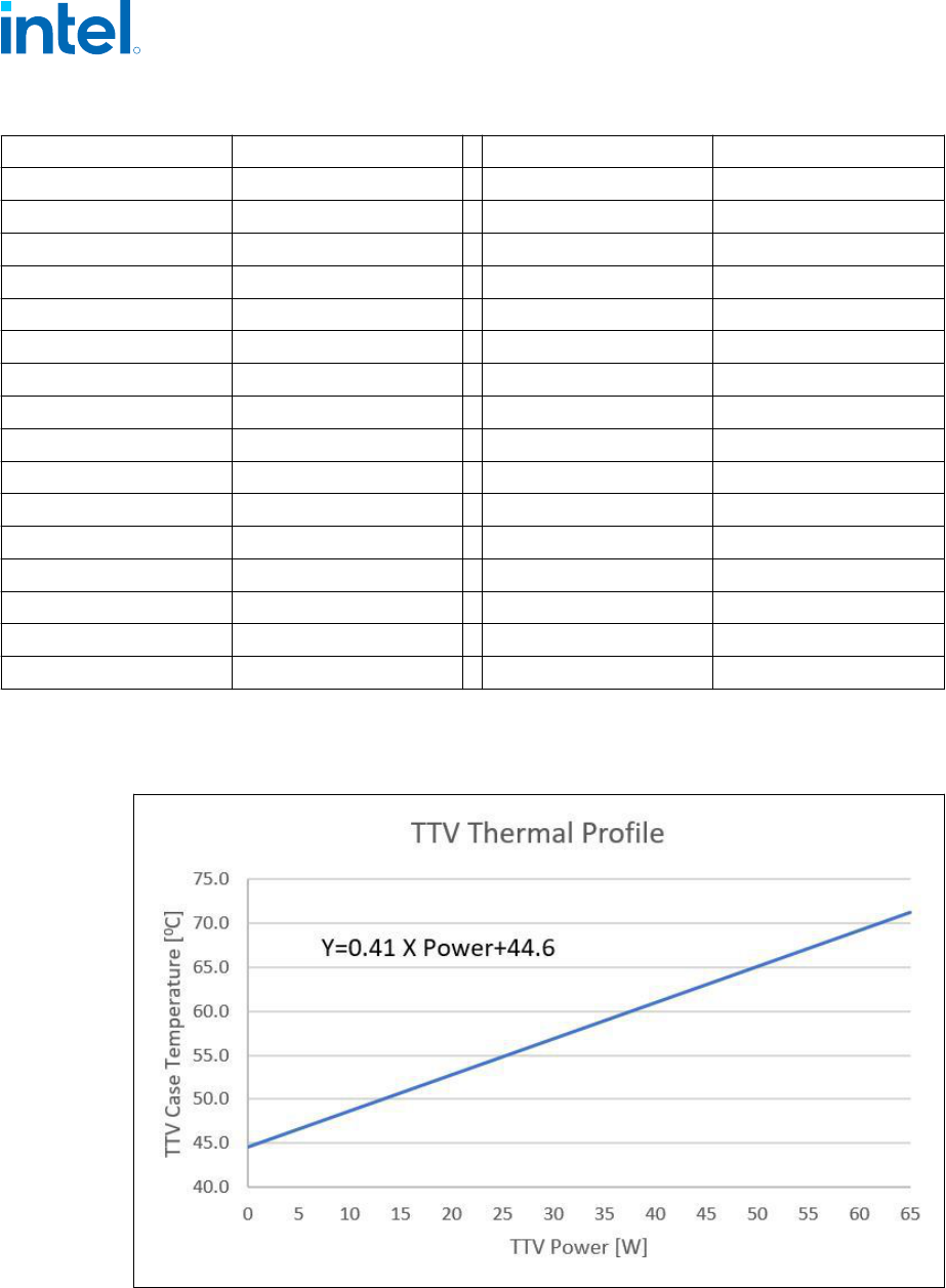
Power (W) T
CASE_MAX
(ºC) Power (W) T
CASE_MAX
(ºC)
32 47.9 96 57.5
34 48.2 98 57.8
36 48.5 100 58.1
38 48.8 102 58.4
40 49.1 104 58.7
42 49.4 106 58.0
44 49.7 108 58.3
46 50.0 110 59.6
48 50.3 112 59.9
50 50.6 114 60.2
52 50.9 116 60.5
54 51.2 118 60.8
56 51.5 120 61.1
58 51.8 122 61.4
60 52.1 124 61.7
62 52.4 125 61.85
Thermal Profile for PCG 2020C Processor
Figure 20. Thermal Profile for PCG 2020C Processor
4.3.3
R
12th Generation Intel
®
Core
™
Processors—Thermal Management
12
th
Generation Intel
®
Core
™
Processors
Datasheet, Volume 1 of 2 February 2023
100 Doc. No.: 655258, Rev.: 010
NOTE
Refer to table below for discrete points that constitute the thermal profile.
Table 24. Thermal Test Vehicle Thermal Profile for PCG 2020C Processor
Power (W) T
CASE_MAX
(ºC) Power (W) T
CASE_MAX
( ºC)
0 44.6 34 58.54
2 45.42 36 59.36
4 46.24 38 60.18
6 47.06 40 61.0
8 47.88 42 61.82
10 48.7 44 62.64
12 49.52 46 63.46
14 50.34 48 64.28
16 51.16 50 65.1
18 51.98 52 65.92
20 52.8 54 66.74
22 53.62 56 67.56
24 54.42 58 68.38
26 55.26 60 69.2
28 56.08 62 70.02
30 56.9 64 70.84
32 57.72 65 71.25
R
Thermal Management—12th Generation Intel
®
Core
™
Processors
12
th
Generation Intel
®
Core
™
Processors
February 2023 Datasheet, Volume 1 of 2
Doc. No.: 655258, Rev.: 010 101
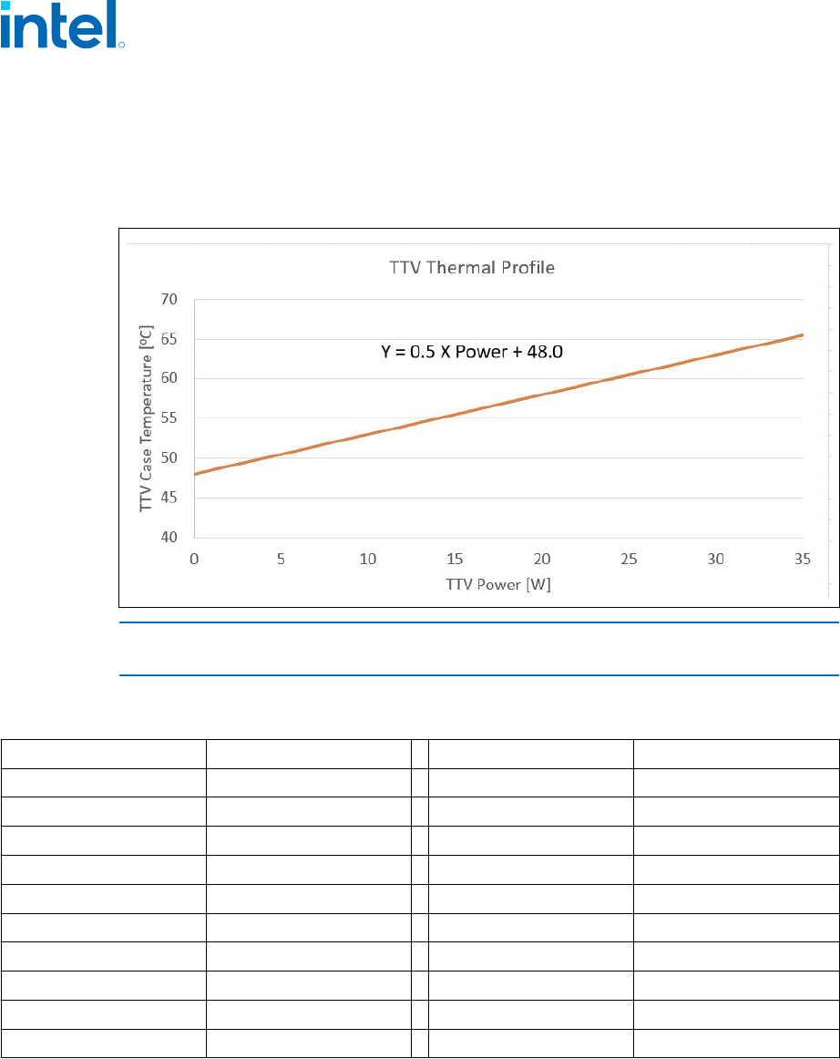
Thermal Profile for PCG 2020D Processor
Thermal Profile for PCG 2020D Processor
Figure 21. Thermal Test Vehicle Thermal Profile for PCG 2020D Processor
NOTE
Refer to table below for discrete points that constitute the thermal profile.
Table 25. Thermal Test Vehicle Thermal Profile for PCG 2020D Processor
Power (W) T
CASE_MAX
(ºC) Power (W) T
CASE_MAX
(ºC)
0 48.0 20 58.0
2 49.0 22 59.0
4 50.0 24 60.0
6 51.0 26 61.0
8 52.0 28 62.0
10 53.0 30 63.0
12 54.0 32 64.0
14 55.0 34 65.0
16 56.0 35 65.5
18 57.0
Thermal Metrology
The maximum TTV case temperatures (T
CASE-MAX
) can be derived from the data in the
appropriate TTV thermal profile earlier in this chapter. The TTV T
CASE
is measured at
the geometric top center of the TTV integrated heat spreader (IHS). Below figure
illustrates the location where T
CASE
temperature measurements should be made.
4.3.4
4.4
R
12th Generation Intel
®
Core
™
Processors—Thermal Management
12
th
Generation Intel
®
Core
™
Processors
Datasheet, Volume 1 of 2 February 2023
102 Doc. No.: 655258, Rev.: 010
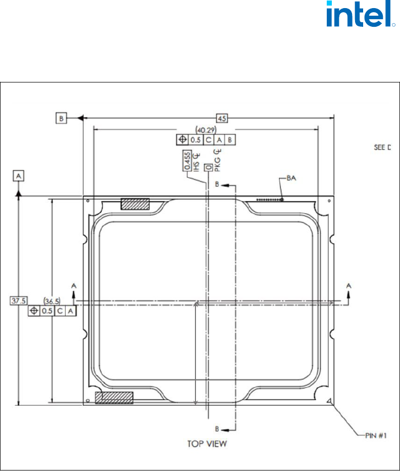
Figure 22. Thermal Test Vehicle (TTV) Case Temperature (T
CASE
) Measurement Location
The following supplier can machine the groove and attach a thermocouple to the IHS.
The following supplier is listed as a convenience to Intel's general customers and may
be subject to change without notice. THERM-X OF CALIFORNIA, 3200 Investment
Blvd, Hayward, Ca 94544. George Landis +1-510-441-7566 Ext. 368 george@therm-
x.com. The vendor part number is XTMS1565.
Fan Speed Control Scheme with DTS
With Digital Thermal Sensor (DTS) 1.1
To correctly use DTS 1.1, the designer must first select a worst case scenario T
AMBIENT
,
and ensure that the Fan Speed Control (FSC) can provide a Ψ CA that is equivalent or
greater than the Ψ CA specification.
The DTS 1.1 implementation consists of two points:
• a Ψ CA at T CONTROL
4.5
R
Thermal Management—12th Generation Intel
®
Core
™
Processors
12
th
Generation Intel
®
Core
™
Processors
February 2023 Datasheet, Volume 1 of 2
Doc. No.: 655258, Rev.: 010 103
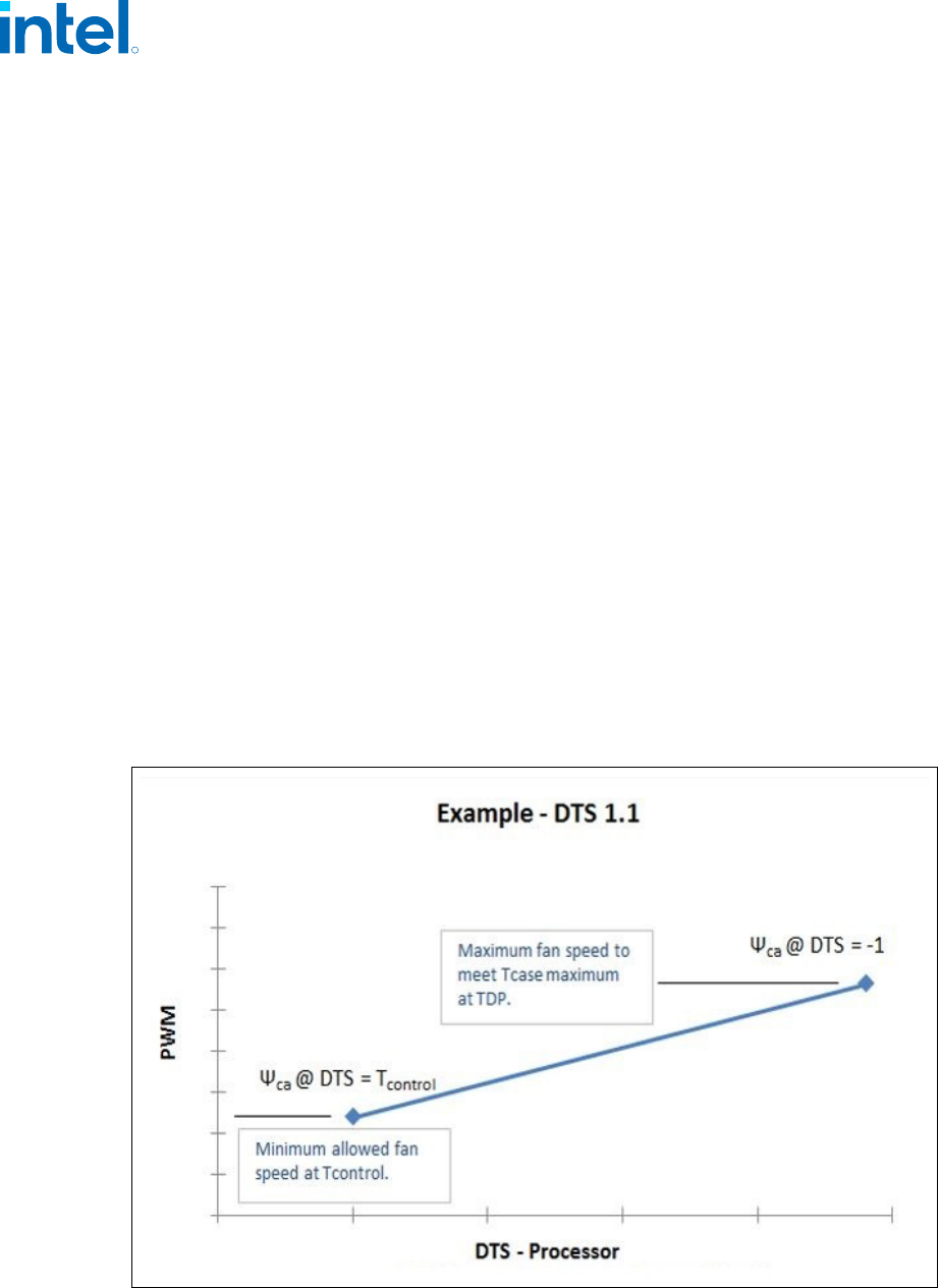
• a Ψ CA at DTS = -1
• The Ψ CA point at DTS = -1 defines the minimum Ψ CA required at Processor Base
Power (a.k.a TDP) considering the worst case system design T
AMBIENT
design
point:
Ψ CA = (T CASE-MAX - T AMBIENT-TARGET - 1 ) / TDP
For example, for a 125 W Processor Base Power (a.k.a TDP) part, the T
CASE
maximum is 62.0 °C and at a worst case design point of 40 °C local ambient this
will result in:
Ψ CA = (62.0 - 40 - 1) / 125 = 0.168 °C/W
Similarly for a system with a design target of 45 °C ambient, the Ψ CA at DTS =
-1 needed will be 0.128 °C/W.
• The second point defines the thermal solution performance (Ψ CA ) at T
CONTROL . The following table lists the required Ψ CA for the various Processor
Base Power (a.k.a TDP) processors.
These two points define the operational limits for the processor for DTS 1.1
implementation. At T CONTROL the fan speed must be programmed such that the
resulting Ψ CA is better than or equivalent to the required Ψ CA listed in the following
table. Similarly, the fan speed should be set at DTS = -1 such that the thermal
solution performance is better than or equivalent to the ΨCA requirements at T
AMBIENT-MAX .
The fan speed controller must linearly ramp the fan speed from processor DTS = T
CONTROL to processor DTS = -1.
Figure 23. Digital Thermal Sensor (DTS) 1.1 Definition Points
R
12th Generation Intel
®
Core
™
Processors—Thermal Management
12
th
Generation Intel
®
Core
™
Processors
Datasheet, Volume 1 of 2 February 2023
104 Doc. No.: 655258, Rev.: 010
Table 26. Digital Thermal Sensor (DTS) 1.1 Thermal Solution Performance Above
T
CONTROL
Processor
Ψ
CA
at DTS =
T
CONTROL
1, 2
At System
T
AMBIENT_MAX
= 30 °C
Ψ
CA
at DTS =
-1
At System
T
AMBIENT_MAX
= 40 °C
Ψ
CA
at DTS =
-1
At System
T
AMBIENT_MAX
= 45 °C
Ψ
CA
at DTS = -1
At System
T
AMBIENT_MAX
= 50 °C
8+8 -Core 150W 0.21 0.12 0.08 0.05
8+8 -Core 125W 0.26 0.16 0.12 0.08
8+4-Core 125W 0.28 0.16 0.12 0.08
6+4 -Core 125W 0.30 0.16 0.12 0.08
8+8-Core 65W 0.64 0.46 0.38 0.31
8+4-Core 65W 0.65 0.46 0.38 0.31
8+8-Core 35W 0.86 0.7 0.55 0.41
6+0-Core 65W 0.72 0.46 0.38 0.31
6+0-Core 35W 0.97 0.7 0.55 0.41
4+0-Core 35W 1.0 0.7 0.55 0.41
4+0-Core 60W 0.77 0.7 0.55 0.41
4+0-Core 58W 0.78 0.7 0.55 0.41
2+0-Core 35W 0.1.18 0.7 0.55 0.41
2+0-Core 46W 0.84 0.7 0.55 0.41
Notes: 1. Ψ
CA
at “DTS = T
CONTROL
” is applicable to systems that have an internal T
RISE
(T
ROOM
temperature to Processor cooling fan inlet) of less than 10 °C. In case the expected T
RISE
is
greater than 10 °C, a correction factor should be used as explained below. For each 1 °C T
RISE
above 10 °C, the correction factor (CF) is defined as CF = 1.7 / (Processor Base Power (a.k.a
TDP)).
2. The table data match for GT0.
With Digital Thermal Sensor (DTS) 2.0
To simplify processor thermal specification compliance, the processor calculates the
DTS Thermal Profile from TCONTROL Offset, TCC Activation Temperature, Processor
Base Power (a.k.a TDP), and the Thermal Margin Slope provided in the following table.
NOTE
TCC Activation Offset is 0 for the processors.
Using the DTS Thermal Profile, the processor can calculate and report the Thermal
Margin, where a value less than 0 indicates that the processor needs additional
cooling, and a value greater than 0 indicates that the processor is sufficiently cooled.
R
Thermal Management—12th Generation Intel
®
Core
™
Processors
12
th
Generation Intel
®
Core
™
Processors
February 2023 Datasheet, Volume 1 of 2
Doc. No.: 655258, Rev.: 010 105
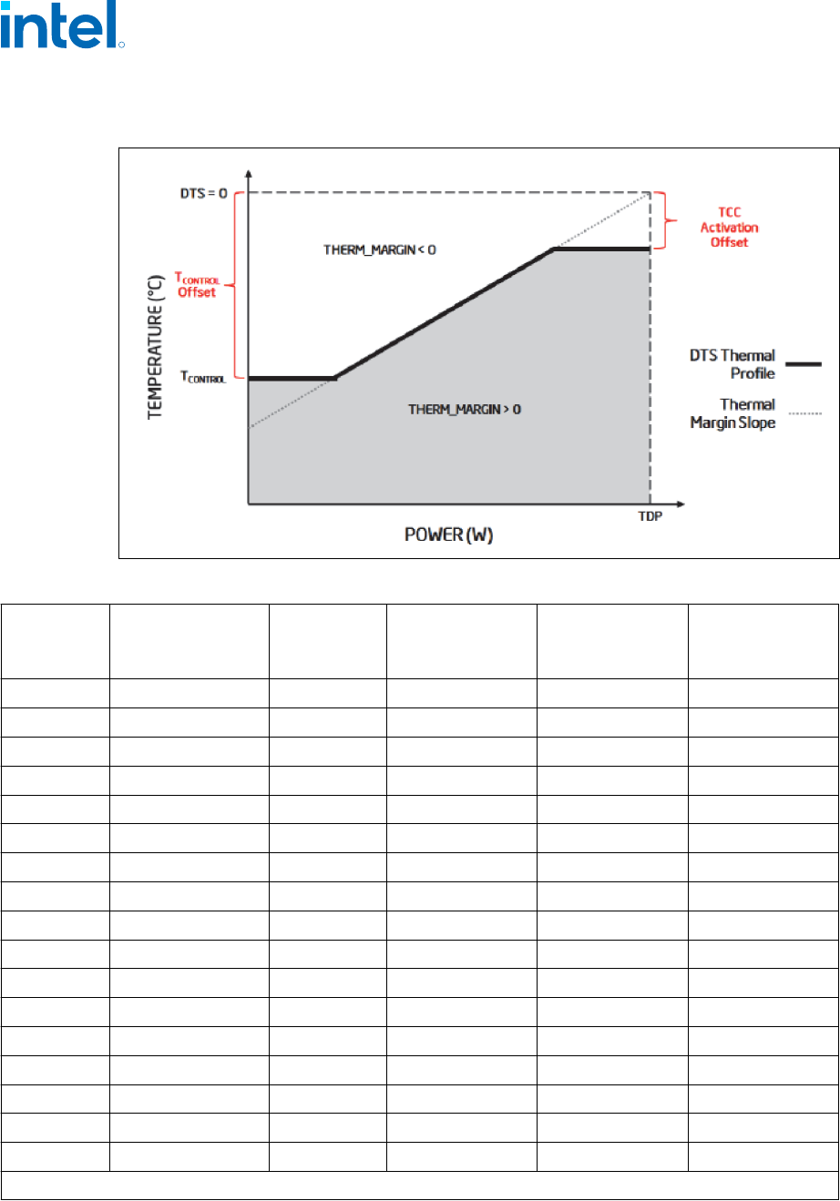
Figure 24. Digital Thermal Sensor (DTS) 2.0 Definition Points
Table 27. Thermal Margin Slope
PCG
Die Configuration
(Cores/GT)
Processor
Base Power
(a.k.a TDP)
[W]
TCC Activation
[°C]
Temperature
Control Offset
Thermal Margin
Slope [°C/W]
2020A 8+8 Core 150 90
1
20 0.32
2020A 8+8 Core 125 100 20 0.35
2020A 8+8 Core GT0 125 100 20 0.36
2020A 8+4 Core 125 100 20 0.38
2020A 8+4 Core GT0 125 100 20 0.39
2020A 6+4 Core 125 100 20 0.44
2020A 6+4 Core GT0 125 100 20 0.45
2020C 8+8 Core 65 100 20 0.59
2020C 8+4 Core 65 100 20 0.61
2020C 6+0 Core 65 100 20 0.77
2020C 4+0 Core 60 100 20 0.92
2020C 4+0 Core 58 100 20 0.96
2020C 2+0 Core 46 100 20 1.24
2020D 8+8 Core 35 100 20 0.68
2020D 6+0 Core 35 100 20 0.84
2020D 4+0 Core 35 100 20 0.95
2020D 2+0 Core 35 100 20 1.26
Note: 1. The default BIOS settings for this SKU is 10C TCC offset.
R
12th Generation Intel
®
Core
™
Processors—Thermal Management
12
th
Generation Intel
®
Core
™
Processors
Datasheet, Volume 1 of 2 February 2023
106 Doc. No.: 655258, Rev.: 010
5.0 Memory
System Memory Interface
Processor SKU Support Matrix
Table 28. DDR Support Matrix Table
Technology DDR4 DDR5 LPDDR4x
LPDDR5/x
15,16
Processor HX / S /
H / P / U15
HX / S HX / S /
H / P / U15
HX / S H/P/U15/U9 H/P/U15/U9
Configuration 1DPC 2DPC
11
1DPC 2DPC
11
1R/2R 1R/2R
Maximum Frequency
[MT/s]
S
UDIMM
3200
HX / S /
H /P / U15
SoDIMM
3200
S
UDIMM 3200
12
HX SoDIMM :
1 DIMM - 2933
12
2 DIMMs -
3200
HX /S / P /
U15
SoDIMM
4800
S :
UDIMM
4800
S UDIMM :
1 DIMM - 4400,
2 DIMMs 1R -
4000,
2 DIMMs 2R - 3600
HX SoDIMM:
1 DIMM - 4000,
2 DIMMs 1R -
4000,
2 DIMMs 2R - 3600
4266 Type4 :
1R/2R :5200
P/H Type3:
1R/2R 4800
VDDQ [V]
6
1.2 5,1.1
10
0.6 0.5
VDD2 [V]
6
1.2 1.1 1.1 1.05
Maximum RPC
2
2 4 2 4 2 2
continued...
5.1
5.1.1
R
Memory—12th Generation Intel
®
Core
™
Processors
12
th
Generation Intel
®
Core
™
Processors
February 2023 Datasheet, Volume 1 of 2
Doc. No.: 655258, Rev.: 010 107
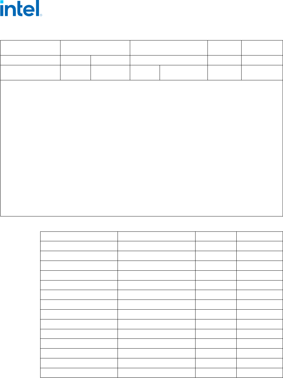
Technology DDR4 DDR5 LPDDR4x
LPDDR5/x
15,16
Die Density [Gb] 8,16 8,16 16 8,16 8, 12
7
,16
Ballmap Mode
11
IL /NIL IL /NIL P : NIL,
HX /S - IL
NIL NIL
NIL
Notes: 1. 1DPC refer to when only 1DIMM slot per channel is routed.
2. RPC = Rank Per Channel
3. An Interleave SoDIMM/MD placements like butterfly or back-to-back supported with a Non-Interleave ballmap
mode at H, P, U15 - Processor Line
4. Memory down of all technologies should be implemented homogeneous means that all DRAM devices should be
from the same vendor and have the same part number. Implementing a mix of DRAM devices may cause
serious signal integrity and functional issues.
5. There is no support for memory modules with different technologies or capacities on opposite sides of the same
memory module. If one side of a memory module is populated, the other side is either identical or empty.
6. VDD2 is Processor and DRAM voltage, and VDDQ is DRAM voltage.
7. Pending DRAM samples availability.
8. Maximum 2DPC frequency supported when same DIMM part number populated Within channel. Frequency is not
guaranteed when mix DIMM's populated.
9. Mix DIMM in 2DPC use 2N Command Mode, speed to be set in BIOS per margin check.
10.5V is SODIMM/UDIMM voltage, 1.1V is Memory down voltage.
11.DDR4/DDR5 SoDIMM 2DPC - Not supported on S -Processor Line.
12.Far memory slot to be populated in case single dimm placed on 2DPC channel
13.IL/NIL mode depends on Memory topology.
14.DDR4/DDR5 ECC is supported only when all memory populated in the system supports ECC.
15.LPDDR5 technology supports 8 Bank Mode, BG (Bank Group) Mode and 16 Bank Mode. This processor supports
8 Bank Mode only.
16.LPDDR5x 1a node Supported from MR5 BKC release under LPDDR5 POR speed and with 8B mode only.
Table 29. DDR Technology Support Matrix
Technology Form Factor Ball Count Processor
DDR4 UDIMM 288 S
DDR4 SoDIMM 260 HX/H/P/U15/S
DDR4 x16 SDP (1R)
1
96 H/P/U15
DDR4 x16 DDP (1R)
1
96 H/P/U15
DDR4 x8 SDP (1R)
1
78 H/P/U15
DDR5 SoDIMM 262 HX/H/P/U15/S
DDR5 UDIMM 288 S
DDR5 x8 SDP (1R)
1
78 H/P/U15
DDR5 x16 SDP (1R)
1
102 H/P/U15
LPDDR4x x32 (1R, 2R)
1
200 H/P/U15/U9
LPDDR4x x64 (1R, 2R)
1
432 H/P/U15/U9
LPDDR4x х64 (1R, 2R)
1
556 U9
LPDDR5/x x64 (1R, 2R)
1
496 H/P/U15/U9
LPDDR5/x x32 (1R, 2R)
1
315 H/P/U15/U9
R
12th Generation Intel
®
Core
™
Processors—Memory
12
th
Generation Intel
®
Core
™
Processors
Datasheet, Volume 1 of 2 February 2023
108 Doc. No.: 655258, Rev.: 010
NOTE
• Memory down of all technologies should be implemented homogeneously, which
means that all DRAM devices should be from the same vendor and have the same
part number. Implementing a mix of DRAM devices may cause serious signal
integrity and functional issues, DDR4/DDR5 restriction is for single MC
configuration, LPDDR4x/LPDDR5/x restriction is for both MC configuration (all
DRAMs in the system must be from same Part Number).
Supported Memory Modules and Devices
Table 30. Supported DDR4 Non-ECC SoDIMM Module Configurations (S/H/P/U15-
Processor Line)
Raw
Card
Version
DIMM
Capacity
DRAM
Device
Technology
DRAM
Organization
# of
DRAM
Devices
# of
Ranks
# of Row/Col
Address Bits
# of Banks
Inside
DRAM
Page
Size
A 8 GB 8 Gb 1024M x 8 8 1 16/10 16 8K
A 16 GB 16 Gb 2048M x 8 8 1 17/10 16 8K
C 4 GB 8 Gb 512M x 16 4 1 16/10 8 8K
C 8 GB 16 Gb 1024M x 16 4 1 17/10 8 8K
E 16 GB 8 Gb 1024M x 8 16 2 16/10 16 8K
E 32 GB 16 Gb 2048M x 8 16 2 17/10 16 8K
Table 31. Supported DDR4 ECC SoDIMM Module Configurations (S-Processor Line)
Raw
Card
Version
DIMM
Capacity
DRAM
Device
Technology
DRAM
Organization
# of
DRAM
Devices
# of
Ranks
# of Row/Col
Address Bits
# of Banks
Inside
DRAM
Page
Size
D 8 GB 8 Gb 1024M x 8 9 1 16/10 16 8K
D 16 GB 16 Gb 2048M x 8 9 1 17/10 16 8K
G 8 GB 8 Gb 1024M x 8 18 2 16/10 16 8K
G 16 GB 16 Gb 2048M x 8 18 2 17/10 16 8K
F 16 GB 8 Gb 1024M x 8 18 2 16/10 16 8K
F 32 GB 16 Gb 2048M x 8 18 2 17/10 16 8K
Table 32. Supported DDR4 Non-ECC UDIMM Module Configurations (S-Processor Line)
Raw
Card
Version
DIMM
Capacity
DRAM
Device
Technology
DRAM
Organization
# of
DRAM
Devices
# of
Ranks
# of Row/Col
Address Bits
# of Banks
Inside
DRAM
Page
Size
A 8 GB 8 Gb 1024M x 8 8 1 16/10 16 8K
A 16 GB 16 Gb 2048M x 8 8 1 17/10 16 8K
C 4 GB 8 Gb 512M x 16 4 1 16/10 8 8K
C 8 GB 16 Gb 1024M x 16 4 1 17/10 8 8K
B 16 GB 8 Gb 1024M x 8 16 2 16/10 16 8K
B 32 GB 16 Gb 2048M x 8 16 2 17/10 16 8K
5.1.2
R
Memory—12th Generation Intel
®
Core
™
Processors
12
th
Generation Intel
®
Core
™
Processors
February 2023 Datasheet, Volume 1 of 2
Doc. No.: 655258, Rev.: 010 109

Table 33. Supported DDR4 ECC UDIMM Module Configurations (S-Processor Line)
Raw
Card
Version
DIMM
Capacity
DRAM
Device
Technology
DRAM
Organization
# of
DRAM
Devices
# of
Ranks
# of Row/Col
Address Bits
# of Banks
Inside
DRAM
Page
Size
D 8 GB 8 Gb 1024M x 8 9 1 16/10 16 8K
D 16 GB 16 Gb 2048M x 8 9 1 17/10 16 8K
E 4 GB 8 Gb 1024M x 8 18 2 16/10 16 8K
E 8 GB 16 Gb 2048M x 8 18 2 17/10 16 8K
Table 34. Supported DDR5 Non-ECC SoDIMM Module Configurations (S/H/P/U15-
Processor Line)
Raw
Card
Version
DIMM
Capacity
DRAM
Device
Technology
DRAM
Organization
# of
DRAM
Devices
# of
Ranks
# of Row/Col
Address Bits
# of Banks
Inside
DRAM
Page
Size
A 16 GB 16 Gb 2048M x 8 8 1 17/10 16 8K
C 8 GB 16 Gb 1024M x 16 4 1 17/10 8 8K
B 32 GB 16 Gb 2048M x 8 16 2 17/10 16 8K
Table 35. Supported DDR5 ECC SoDIMM Module Configurations (S-Processor Line)
Raw
Card
Version
DIMM
Capacity
DRAM
Device
Technology
DRAM
Organization
# of
DRAM
Devices
# of
Ranks
# of Row/Col
Address Bits
# of Banks
Inside
DRAM
Page
Size
D 16 GB 16 Gb 2048M x 8 9 1 17/10 16 8K
E 32 GB 16 Gb 2048M x 8 18 2 17/10 16 8K
Table 36. Supported DDR5 Non-ECC UDIMM Module Configurations (S-Processor Line)
Raw
Card
Version
DIMM
Capacity
DRAM
Device
Technology
DRAM
Organization
# of
DRAM
Devices
# of
Ranks
# of Row/Col
Address Bits
# of Banks
Inside
DRAM
Page
Size
A 16 GB 16 Gb 2048M x 8 8 1 17/10 16 8K
C 8 GB 16 Gb 1024M x 16 4 1 17/10 8 8K
B 32 GB 16 Gb 2048M x 8 16 2 17/10 16 8K
Table 37. Supported DDR5 ECC UDIMM Module Configurations (S-Processor Line)
Raw
Card
Version
DIMM
Capacity
DRAM
Device
Technology
DRAM
Organization
# of
DRAM
Devices
# of
Ranks
# of Row/Col
Address Bits
# of Banks
Inside
DRAM
Page
Size
D 16 GB 16 Gb 2048M x 8 9 1 17/10 16 8K
E 32 GB 16 Gb 2048M x 8 18 2 17/10 16 8K
R
12th Generation Intel
®
Core
™
Processors—Memory
12
th
Generation Intel
®
Core
™
Processors
Datasheet, Volume 1 of 2 February 2023
110 Doc. No.: 655258, Rev.: 010
Table 38. Supported DDR4 Memory Down Device Configurations (H/P /U15 Processor
Line)
Maximum
System
Capacity
3
PKG
Type
(Die
bits x
Packag
e bits)
DRAM
Organizat
ion /
Package
Type
Packag
e
Density
Die
Density
Dies
Per
Channel
Rank
Per
Channel
PKGs
Per
Channel
Physica
l Device
Rank
Banks
Inside
DRAM
Page
Size
32 GB SDP 8x8 1024M x 8 8 Gb 8 Gb 16 2 16 1 16 8K
64 GB SDP 8x8 2048M x 8 16 Gb 16 Gb 16 2 16 1 16 8K
8 GB
SDP
16x16
512M x 16 8 Gb 8 Gb 4 1 4 1 8 8K
16 GB
1
SDP
16x16
1024M x
16
16 Gb 16 Gb 4 1 4 1 8 8K
16 GB
DDP
8x16
1024M x
16
16 Gb 8 Gb 8 1 4 1 16 8K
32 GB
2
DDP
8x16
2048M x
16
32 Gb 16 Gb 8 1 4 1 16 8K
Notes: 1. For SDP: 1Rx16 using 16 GB die density - the maximum system capacity is 16 GB
2. For DDP: 1Rx16 using 16 GB die density - the maximum system capacity is 32 GB.
3. Maximum system capacity refer to system with 2 channels populated
Table 39. Supported DDR5 Memory Down Device Configurations (H/P/U15 Processor
Line)
Maximu
m
System
Capacit
y
3
PKG
Type
(Die
bits x
Packag
e bits)
DRAM
Organizat
ion /
Package
Type
Packag
e
Density
Die
Density
Dies
Per
Channel
Rank
Per
Channel
PKGs
Per
channel
Physical
Device
Rank
Banks
Inside
DRAM
Page
Size
32 GB SDP 8x8 2048M x 8 16 Gb 16 Gb 8 1 8 1 16 8K
16 GB
1
SDP
16x16
1024M x
16
16 Gb 16 Gb 4 1 4 1 8 8K
Notes: 1. For SDP: 1Rx16 using 16 GB die density - the maximum system capacity is 16 GB
2. Maximum system capacity, refer to system with 2 channels populated
Table 40. Supported LPDDR4x x32 DRAMs Configurations (H/P/U Processor Line)
Maximum System
Capacity
4
PKG
Type
(Die bits per Ch x PKG
bits)
2
Die Density PKG Density
Rank Per
PKGs
8 GB DDP 16x32 8 Gb 16 Gb 1
16 GB QDP 16x32 8 Gb 32 Gb 2
32 GB ODP 16x32(Byte mode) 8 Gb 64 Gb 2
16 GB QDP 16x32 16 Gb 32 Gb 1
32 GB ODP 16x32 16 Gb 64 Gb 2
Notes: 1. x32 BGA devices are 200 balls
2. QDP = Quad Die Package, ODP-Octal Die Package
3. Each LPDDR4x channel include two sub-channels
4. Maximum system capacity refers to system with all 8 sub channels populated
R
Memory—12th Generation Intel
®
Core
™
Processors
12
th
Generation Intel
®
Core
™
Processors
February 2023 Datasheet, Volume 1 of 2
Doc. No.: 655258, Rev.: 010 111
Table 41. Supported LPDDR4x x64 DRAMs Configurations (H/P/U Processor Line)
Maximum
System
Capacity
3
PKG Type
(Die bits
per Ch x
PKG bits)
Die
Density
Ball Count
Per PKG
PKG
Density
DRAM
Channels
Per PKGs
Processor
Line
Rank Per
PKGs
8 GB QDP 16x64 8 Gb 432 32 Gb 4 H/P/U 1
16 GB ODP 16x64 8 Gb 432 64 Gb 4 H/P/U 2
16 GB QDP 16x64 16 Gb 432 64 Gb 4 H/P/U 2
8 GB QDP 16x64 8 Gb 556 32 Gb 4 U9 1
16 GB ODP 16x64 8 Gb 556 64 Gb 4 U9 2
16 GB QDP 16x64 16 Gb 556 64 Gb 4 U9 2
Notes: 1. QDP = Quad Die Package, ODP-Octal Die Package
2. Each LPDDR4x channel include two sub-channels
3. Maximum system capacity refers to system with all 8 sub-channels populated
Table 42. Supported LPDDR5/x x32 DRAMs Configurations
6
(H/P/U Processor Line)
Maximum System
Capacity
4
PKG
Type
(Die bits per Ch x PKG
bits)
2
Die Density PKG Density
Rank Per
PKGs
12 GB
5
DDP 16x32 12 Gb 24 Gb 1
24 GB
5
QDP 16x32 12 Gb 48 Gb 2
16 GB DDP 16x32 16 Gb 32 Gb 1
32 GB QDP 16x32 16 Gb 64 Gb 2
64 GB
5
ODP 16x32 16 Gb 128 Gb 2
8 GB DDP 16x32 8 Gb 16 Gb 1
16 GB QDP 16x32 8 Gb 32 Gb 2
32 GB ODP 16x32 8 Gb 64 Gb 2
Notes: 1. x32 BGA devices are 315 balls
2. QDP = Quad Die Package, ODP-Octal Die Package
3. Each LPDDR5 channel include two sub-channels
4. Maximum system capacity refers to system with all 8 sub channels populated
5. Pending DRAM samples availability.
6. LPDDR5x supported with 1a node only.
Table 43. Supported LPDDR5/x x64 DRAMs Configurations
4
(H/P/U Processor Line)
Maximum System
Capacity
3
PKG
Type
(Die bits per Ch x
PKG bits)
Die
Density
PKG Density
DRAM
Channels
Per PKGs
Rank Per
PKGs
16 GB QDP 16x64 16 Gb 64 Gb 4 1
32 GB ODP 16x64 16 Gb 128 Gb 4 2
8 GB QDP 16x64 8 Gb 32 Gb 4 1
16 GB ODP 16x64 8 Gb 64 Gb 4 2
Notes: 1. QDP = Quad Die Package, ODP-Octal Die Package
2. Each LPDDR5 channel include two sub-channels
3. Maximum system capacity refers to system with all 8 sub-channels populated
4. LPDDR5x supported with 1a node only.
R
12th Generation Intel
®
Core
™
Processors—Memory
12
th
Generation Intel
®
Core
™
Processors
Datasheet, Volume 1 of 2 February 2023
112 Doc. No.: 655258, Rev.: 010
System Memory Timing Support
The IMC supports the following DDR Speed Bin, CAS Write Latency (CWL), and
command signal mode timings on the main memory interface:
• tCL = CAS Latency
• tRCD = Activate Command to READ or WRITE Command delay
• tRP = PRECHARGE Command Period
• tRPb = per-bank PRECHARGE time
• tRPab = all-bank PRECHARGE time
• CWL = CAS Write Latency
• Command Signal modes:
— 2N indicates a new DDR5/DDR4/LPDDR4x/LPDDR5/x command may be issued
every 2 clocks.
— 1N indicates a new DDR5/DDR4/LPDDR4x/LPDDR5/x command may be issued
every clock.
System Memory Timing Support
Table 44. DDR System Memory Timing Support
DRAM
Device
Transfer
Rate
(MT/s)
tCL (tCK) tRCD (ns) tRP (ns) CWL (tCK) DPC
CMD
Mode
DDR4 3200 22 13.75 13.75
9-12,
14,16,18,20
1,2 2N
DDR5
4000 36 17 17.00 34 1 2N
4400 40 16.82 16.82 38 1,2
1
2N
4800 40 16.67 16.67 38 1 2N
Note:
1. 2 DPC supported when one slot is populated in each channel
2. Support 8 Bank Mode ( 8B ) only
Table 45. LPDDR System Memory Timing Support
DRAM
Device
Transfer Rate
(MT/s)
tCL (tCK) tRCD (ns) tRPpb (ns) tRPab (ns)
WL (tCK)
Set B
LPDDR4x 4266 36 18 18 21 34
LPDDR5/x
4800 13 18.33 18.33 21.67 12
5200 15 18.46 18.46 21.54 14
Note:
1. Support 8 Bank Mode ( 8B ) only
SAGV Points
SAGV (System Agent Geyserville) is a way by which they SoC can dynamically scale
the work point (V/F), by applying DVFS (Dynamic Voltage Frequency Scaling) based
on memory bandwidth utilization and/or the latency requirement of the various
5.1.3
5.1.3.1
5.1.3.2
R
Memory—12th Generation Intel
®
Core
™
Processors
12
th
Generation Intel
®
Core
™
Processors
February 2023 Datasheet, Volume 1 of 2
Doc. No.: 655258, Rev.: 010 113
workloads for better energy efficiency at System-Agent. Pcode heuristics are in charge
of providing request for Qclock work points by periodically evaluating the utilization of
the memory and IA stalls.
Table 46. SA Speed Enhanced Speed Steps (SA-GV) and Gear Mode Frequencies
Technology
DDR Maximum
Rate [MT/s]
SAGV-
LowBW
SAGV-MedBW SAGV-HighBW
SAGV-
MaxBW/
lowest latency
S/HX-
Processor
DDR4 3200 2133 G2 2666 G1 2933 G1 3200 G1
DDR5 1DPC 4800 2000 G2 3600 G2 4400 G2 4800 G2
DDR5 1DPC on
2DPC SODIMM
4000 2000 G2 3600 G2 3600 G2 4000 G2
DDR5 1DPC on
2DPC UDIMM (S
only)
4400 2000 G2 3600 G2 4000 G2 4400 G2
DDR5 2DPC
1R/1R
4000 2000 G2 3600 G2 3600 G2 4000 G2
DDR5 2DPC
2R/2R
3600 2000 G2 3200 G2 3200 G2 3600 G2
H-Processor
LPDDR4x 4266 2666 G4 3733 G4 4266 G4 4266 G2
LPDDR5/x
1R/2R
3
5200 2400 G4 4800 G4 5200 G4 5200 G2
LPDDR5/x
1R/2R
4800 2400 G4 4400 G4 4400 G4 4800 G2
DDR4 3200 2133 G2 2933 G2 3200 G2 2666 G1
DDR5 4800 2000 G2 3600 G2 4400 G2 4800 G2
P/U15-
Processor
LPDDR4x 4266 2666 G4 3733 G4 4266 G4 4266 G2
LPDDR5/x
1R/2R
3
5200 2400 G4 4800 G4 5200 G4 5200 G2
LPDDR5/x
1R/2R
4800 2400 G4 4400 G4 4800 G4 4800 G2
DDR4 3200 2133 G2 2933 G2 3200 G2 2666 G1
DDR5 4800 2000 G2 4400 G4 4800 G4 4800 G2
U9-Processor
LPDDR4x 4266 2666 G4 3733 G4 4266 G4 4266 G2
LPDDR5/x
1R/2R
5200 2400 G4 4800 G4 5200 G4 5200 G2
Notes: 1. 12th Generation Intel
®
Core
™
Processors supports dynamic gearing technology where the Memory Controller
can run at 1:1 (Gear-1, Legacy mode) or 1:2 (Gear-2 mode) and 1:4 (Gear-4 mode) ratio of DRAM speed. The
gear ratio is the ratio of DRAM speed to Memory Controller Clock.
MC Channel Width equal to DDR Channel width multiply by Gear Ratio
2. Type 4 board only.
3. SAGV is not supported on S 125W Processors.
4. SA-GV modes
a. LowBW- Low frequency point, Minimum Power point. Characterized by low power, low BW, high latency. The
system will stay at this point during low to moderate BW consumption.
b. MedBW - Tuned for balance between power & performance
c. HighBW Characterized by high power, low latency, moderate BW also used as RFI mitigation point.
d. MaxBW/ lowest latency Lowest Latency point, low BW and highest power.
R
12th Generation Intel
®
Core
™
Processors—Memory
12
th
Generation Intel
®
Core
™
Processors
Datasheet, Volume 1 of 2 February 2023
114 Doc. No.: 655258, Rev.: 010

DDR Frequency Shifting
DDR interfaces emit electromagnetic radiation which can couple to the antennas of
various radios that are integrated in the system, and cause radio frequency
interference (RFI).
The DDR Radio Frequency Interference Mitigation (DDR RFIM) feature is primarily
aimed at resolving narrowband RFI from DDR4/5 and LPDDR4x/5/5x technologies for
the Wi-Fi* high and ultra-high bands (~5-7 GHz) .
By changing the DDR data rate, the harmonics of the clock can be shifted out of a
radio band of interest, thus mitigating RFI to that radio. This feature is working with
SAGV on, the 3
rd
SAGV point is used as RFI mitigation point.
Memory Controller (MC)
The integrated memory controller is responsible for transferring data between the
processor and the DRAM as well as the DRAM maintenance. There are two instances of
MC, one per memory slice. Each controller is capable of supporting up to four channels
of LPDDR4x and LPDDR5/x, two channels of DDR5 and one channel of DDR4.
The two controllers are independent and have no means of communicating with each
other, they need to be configured separately.
In a symmetric memory population, each controller only view half of the total physical
memory address space.
Both MC support only one technology in a system DDR4, DDR5, LPDDR4X, or
LPDDR5/x. Mix of technologies in one system is not allowed.
Memory Controller Power Gate
Memory Controller Power Gating can only be done for MC0 which is connected to a
separate power domain. MC0 will be gated automatically when it is not occupied.
NOTE
MC1 cannot be gated.
System Memory Controller Organization Mode (DDR4/5 Only)
The IMC supports two memory organization modes, single-channel and dual-channel.
Depending upon how the DDR Schema and DIMM Modules are populated in each
memory channel, a number of different configurations can exist.
Single-Channel Mode
In this mode, all memory cycles are directed to a single channel. Single-Channel mode
is used when either the Channel A or Channel B DIMM connectors are populated in any
order, but not both.
Dual-Channel Mode – Intel
®
Flex Memory Technology Mode
The IMC supports Intel Flex Memory Technology Mode. Memory is divided into a
symmetric and asymmetric zone. The symmetric zone starts at the lowest address in
each channel and is contiguous until the asymmetric zone begins or until the top
5.1.3.3
5.1.4
5.1.5
5.1.6
R
Memory—12th Generation Intel
®
Core
™
Processors
12
th
Generation Intel
®
Core
™
Processors
February 2023 Datasheet, Volume 1 of 2
Doc. No.: 655258, Rev.: 010 115
address of the channel with the smaller capacity is reached. In this mode, the system
runs with one zone of dual-channel mode and one zone of single-channel mode,
simultaneously, across the whole memory array.
NOTE
Channels A and B can be mapped for physical channel 0 and 1 respectively or vice
versa; however, channel A size should be greater or equal to channel B size.
Figure 25. Intel
®
DDR4/5 Flex Memory Technology Operations
MC BMC A
B B
C
B
B
C
Non interleaved
access
Dual channel
interleaved access
TOM
MC A and MC B can be configured to be physical channels 0 or 1
B – The largest physical memory amount of the smaller size memory module
C – The remaining physical memory amount of the larger size memory module
Dual-Channel Symmetric Mode (Interleaved Mode)
Dual-Channel Symmetric mode, also known as interleaved mode, provides maximum
performance on real world applications. Addresses are ping-ponged between the
channels after each cache line (64-byte boundary). If there are two requests, and the
second request is to an address on the opposite channel from the first, that request
can be sent before data from the first request has returned. If two consecutive cache
lines are requested, both may be retrieved simultaneously, since they are ensured to
be on opposite channels. Use Dual-Channel Symmetric mode when both Channel A
and Channel B DIMM connectors are populated in any order, with the total amount of
memory in each channel being the same.
R
12th Generation Intel
®
Core
™
Processors—Memory
12
th
Generation Intel
®
Core
™
Processors
Datasheet, Volume 1 of 2 February 2023
116 Doc. No.: 655258, Rev.: 010

When both channels are populated with the same memory capacity and the boundary
between the dual channel zone and the single channel zone is the top of memory, IMC
operates completely in Dual-Channel Symmetric mode.
NOTES
• The DRAM device technology and width may vary from one channel to another.
• Different memory size between channels are relevant to DDR4 and DDR5 only.
System Memory Frequency
In all modes, the frequency of system memory is the lowest frequency and latency of
all memory modules placed in the system, as determined through the SPD registers
on the memory modules. The system memory controller supports a single DIMM
connector per channel. If DIMMs with different latency are populated across the
channels, the BIOS will use the slower of the two latencies for both channels. For
Dual-Channel modes, both channels should have a DIMM connector populated. For
Single-Channel mode, only a single channel can have a DIMM connector populated.
Technology Enhancements of Intel
®
Fast Memory Access (Intel
®
FMA)
The following sections describe the Just-in-Time Scheduling, Command Overlap, and
Out-of-Order Scheduling Intel FMA technology enhancements.
Just-in-Time Command Scheduling
The memory controller has an advanced command scheduler where all pending
requests are examined simultaneously to determine the most efficient request to be
issued next. The most efficient request is picked from all pending requests and issued
to system memory Just-in-Time to make optimal use of Command Overlapping. Thus,
instead of having all memory access requests go individually through an arbitration
mechanism forcing requests to be executed one at a time, they can be started without
interfering with the current request allowing for concurrent issuing of requests. This
allows for optimized bandwidth and reduced latency while maintaining appropriate
command spacing to meet system memory protocol.
Command Overlap
Command Overlap allows the insertion of the DRAM commands between the Activate,
Pre-charge, and Read/Write commands normally used, as long as the inserted
commands do not affect the currently executing command. Multiple commands can be
issued in an overlapping manner, increasing the efficiency of system memory protocol.
Out-of-Order Scheduling
While leveraging the Just-in-Time Scheduling and Command Overlap enhancements,
the IMC continuously monitors pending requests to system memory for the best use of
bandwidth and reduction of latency. If there are multiple requests to the same open
page, these requests would be launched in a back to back manner to make optimum
use of the open memory page. This ability to reorder requests on the fly allows the
IMC to further reduce latency and increase bandwidth efficiency.
5.1.7
5.1.8
R
Memory—12th Generation Intel
®
Core
™
Processors
12
th
Generation Intel
®
Core
™
Processors
February 2023 Datasheet, Volume 1 of 2
Doc. No.: 655258, Rev.: 010 117

Data Scrambling
The system memory controller incorporates a Data Scrambling feature to minimize the
impact of excessive di/dt on the platform system memory VRs due to successive 1s
and 0s on the data bus. Past experience has demonstrated that traffic on the data bus
is not random and can have energy concentrated at specific spectral harmonics
creating high di/dt which is generally limited by data patterns that excite resonance
between the package inductance and on die capacitances. As a result, the system
memory controller uses a data scrambling feature to create pseudo-random patterns
on the system memory data bus to reduce the impact of any excessive di/dt.
Data Swapping
By default, the processor supports on-board data swapping in two manners (for all
segments and DRAM technologies): Bit swapping is allowed within each Byte for all
DDR technologies.
Bit swapping is allowed within each Byte for all DDR technologies.
LPDDR4x
• x16 sub-channels can be swizzled within their x32 channel
• x32 channels can be swizzled within their x64 MC
LPDDR5/x
• x16 sub-channels can be swizzle within their x64 MC
DDR4: Byte swapping is allowed within each x64 Channel.
DDR5: Byte swapping is allowed within each x32 Channel
ECC bits swap is allowed within ECC byte/nibble: DDR4 ECC[7..0] and DDR5
ECC[3..0].
LPDDR5/x Ascending and Descending
LPDDR5/x support Ascending / descending that swap CA and CS signals connectivity
order.
Ascending
Descending
CA6 CA0
CA5 CA1
CA4 CS_1
CA3 CS_0
CA2 CA2
CS_0 CA3
CS_1 CA4
CA1 CA5
CA0 CA6
5.1.9
5.1.10
5.1.11
R
12th Generation Intel
®
Core
™
Processors—Memory
12
th
Generation Intel
®
Core
™
Processors
Datasheet, Volume 1 of 2 February 2023
118 Doc. No.: 655258, Rev.: 010
NOTE
Ascending / descending can be performed in every x16 sub channel.
LPDDR4x CMD Mirroring
LPDDR4x support Mirroring that swap CA signals connectivity order.
Default Mirrored
CA 0 CA 5
CA 1 CA 4
CA 2 CA 3
CA 3 CA 2
CA 4 CA 1
CA 5 CA 0
NOTE
Mirroring can be performed in every x16 sub channel
DDR I/O Interleaving
NOTE
The processor supports I/O interleaving, which has the ability to swap DDR bytes for
routing considerations. BIOS configures the I/O interleaving mode before DDR
training. H /P/U-Processor line packages are optimized only for Non-Interleaving mode
(NIL).
There are two supported modes:
• Interleave (IL)
• Non-Interleave (NIL)
The following table and figure describe the pin mapping between the IL and NIL
modes.
Table 47. Interleave (IL) and Non-Interleave (NIL) Modes Pin Mapping
IL (DDR4) NIL (DDR4) DDR5 NIL(LPDDR4x) NIL(LPDDR5/x)
Channel Byte Channel Byte Channel Byte Channel Byte Channel Byte
DDR0 Byte0 DDR0 Byte0 DDR0 Byte0 DDR0 Byte0 DDR0 Byte0
DDR0 Byte1 DDR0 Byte1 DDR0 Byte1 DDR0 Byte1 DDR0 Byte1
DDR0 Byte2 DDR0 Byte4 DDR1 Byte0 DDR2 Byte0 DDR2 Byte0
DDR0 Byte3 DDR0 Byte5 DDR1 Byte1 DDR2 Byte1 DDR2 Byte1
continued...
5.1.12
5.1.13
R
Memory—12th Generation Intel
®
Core
™
Processors
12
th
Generation Intel
®
Core
™
Processors
February 2023 Datasheet, Volume 1 of 2
Doc. No.: 655258, Rev.: 010 119
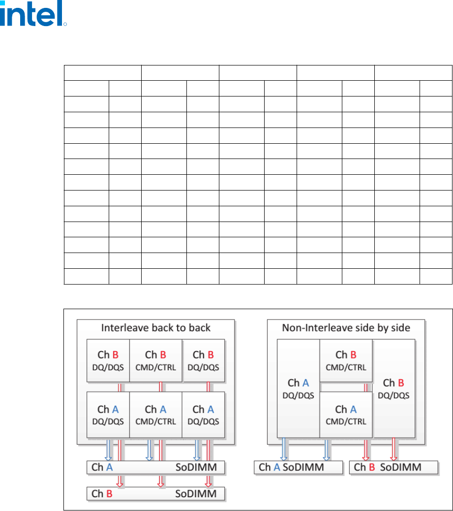
IL (DDR4) NIL (DDR4) DDR5 NIL(LPDDR4x) NIL(LPDDR5/x)
Channel Byte Channel Byte Channel Byte Channel Byte Channel Byte
DDR0 Byte4 DDR1 Byte0 DDR2 Byte0 DDR4 Byte0 DDR4 Byte0
DDR0 Byte5 DDR1 Byte1 DDR2 Byte1 DDR4 Byte1 DDR4 Byte1
DDR0 Byte6 DDR1 Byte4 DDR3 Byte0 DDR6 Byte0 DDR6 Byte0
DDR0 Byte7 DDR1 Byte5 DDR3 Byte1 DDR6 Byte1 DDR6 Byte1
DDR1 Byte0 DDR0 Byte2 DDR0 Byte2 DDR1 Byte0 DDR1 Byte0
DDR1 Byte1 DDR0 Byte3 DDR0 Byte3 DDR1 Byte1 DDR1 Byte1
DDR1 Byte2 DDR0 Byte6 DDR1 Byte2 DDR3 Byte0 DDR3 Byte0
DDR1 Byte3 DDR0 Byte7 DDR1 Byte3 DDR3 Byte1 DDR3 Byte1
DDR1 Byte4 DDR1 Byte2 DDR2 Byte2 DDR5 Byte0 DDR5 Byte0
DDR1 Byte5 DDR1 Byte3 DDR2 Byte3 DDR5 Byte1 DDR5 Byte1
DDR1 Byte6 DDR1 Byte6 DDR3 Byte2 DDR7 Byte0 DDR7 Byte0
DDR1 Byte7 DDR1 Byte7 DDR3 Byte3 DDR7 Byte1 DDR7 Byte1
Figure 26. DDR4 Interleave (IL) and Non-Interleave (NIL) Modes Mapping
DRAM Clock Generation
Each support rank has a differential clock pair for DDR4/5. Each sub-channel has a
differential clock pair for LPDDR4x. Each sub-channel has a (CK_P/N and WCK_P/N)
differential clock pair for LPDDR5/x.
DRAM Reference Voltage Generation
Read Vref is generated by the memory controller in all technologies. Write Vref is
generated by the DRAM in all technologies. Command Vref is generated by the DRAM
in LPDDR4x/LPDDR5/x.
5.1.14
5.1.15
R
12th Generation Intel
®
Core
™
Processors—Memory
12
th
Generation Intel
®
Core
™
Processors
Datasheet, Volume 1 of 2 February 2023
120 Doc. No.: 655258, Rev.: 010

The memory controller generates VrefCA per DIMM for DDR4. In all cases, it has small
step sizes and is trained by MRC.
Data Swizzling
All Processor Lines does not have die-to-package DDR swizzling.
Error Correction With Standard RAM
In-Band error-correcting code (IBECC) correct single-bit memory errors in standard,
non-ECC memory.
Supported only in Chrome systems.
Post Package Repair (PPR)
PPR is supported according to Jedec Spec.
BIOS can identify a single Row failure per Bank in DRAM and perform Post Package
Repair (PPR) to exchange failing Row with spare Row.
PPR can be supported only with DRAM that supports PPR according to Jedec spec.
Supported technologies : DDR4, LPDDR4x, DDR5 and LPDDR5/x.
Integrated Memory Controller (IMC) Power Management
The main memory is power managed during normal operation and in low-power ACPI
C-states.
Disabling Unused System Memory Outputs
Any system memory (SM) interface signal that goes to a memory in which it is not
connected to any actual memory devices (such as SODIMM connector is unpopulated,
or is single-sided) is tri-stated. The benefits of disabling unused SM signals are:
• Reduced power consumption.
• Reduced possible overshoot/undershoot signal quality issues seen by the
processor I/O buffer receivers caused by reflections from potentially unterminated
transmission lines.
When a given rank is not populated, the corresponding control signals (CLK_P/
CLK_N/CKE/ODT/CS) are not driven.
At reset, all rows should be assumed to be populated, until it can be proven that they
are not populated. This is due to the fact that when CKE is tri-stated with a DRAMs
present, the DRAMs are not ensured to maintain data integrity. CKE tri-state should be
enabled by BIOS where appropriate, since at reset all rows should be assumed to be
populated.
DRAM Power Management and Initialization
The processor implements extensive support for power management on the memory
interface. Each channel drives 4 CKE pins, one per rank.
5.1.16
5.1.17
5.1.18
5.2
5.2.1
5.2.2
R
Memory—12th Generation Intel
®
Core
™
Processors
12
th
Generation Intel
®
Core
™
Processors
February 2023 Datasheet, Volume 1 of 2
Doc. No.: 655258, Rev.: 010 121

The CKE is one of the power-saving means. When CKE is off, the internal DDR clock is
disabled and the DDR power is reduced. The power-saving differs according to the
selected mode and the DDR type used. For more information, refer to the IDD table in
the DDR specification.
The processor supports four different types of power-down modes in package C0
state. The different power-down modes can be enabled through configuring PM PDWN
config register. The type of CKE power-down can be configured through PDWN_mode
(bits 15:12) and the idle timer can be configured through PDWN_idle_counter (bits
11:0).
The different power-down modes supported are:
• No power-down: (CKE disable)
• Active Power-down (APD): This mode is entered if there are open pages when
de-asserting CKE. In this mode the open pages are retained. Power-saving in this
mode is the lowest. Power consumption of DDR is defined by IDD3P. Exiting this
mode is fined by tXP – a small number of cycles.
• Pre-charged Power-down (PPD): This mode is entered if all banks in DDR are
pre-charged when de-asserting CKE. Power-saving in this mode is intermediate –
better than APD. Power consumption is defined by IDD2P. Exiting this mode is
defined by tXP. The difference from APD mode is that when waking-up, all page-
buffers are empty.)
The CKE is determined per rank, whenever it is inactive. Each rank has an idle
counter. The idle-counter starts counting as soon as the rank has no accesses, and if it
expires, the rank may enter power-down while no new transactions to the rank arrive
to queues. The idle-counter begins counting at the last incoming transaction arrival. It
is important to understand that since the power-down decision is per rank, the IMC
can find many opportunities to power down ranks, even while running memory
intensive applications; the savings are significant (may be few Watts, according to
DDR specification). This is significant when each channel is populated with more
ranks.
Selection of power modes should be according to power-performance or a thermal
trade-off of a given system:
• When trying to achieve maximum performance and power or thermal
consideration is not an issue: use no power-down
• In a system which tries to minimize power-consumption, try using the deepest
power-down mode possible
• In high-performance systems with dense packaging (that is, tricky thermal
design) the power-down mode should be considered in order to reduce the heating
and avoid DDR throttling caused by the heating.
The idle timer expiration count defines the # of DCLKs that a rank is idle that causes
entry to the selected power mode. As this timer is set to a shorter time the IMC will
have more opportunities to put the DDR in power-down. There is no BIOS hook to set
this register. Customers choosing to change the value of this register can do it by
changing it in the BIOS. For experiments, this register can be modified in real time if
BIOS does not lock the IMC registers.
R
12th Generation Intel
®
Core
™
Processors—Memory
12
th
Generation Intel
®
Core
™
Processors
Datasheet, Volume 1 of 2 February 2023
122 Doc. No.: 655258, Rev.: 010

Initialization Role of CKE
During power-up, CKE is the only input to the SDRAM that has its level recognized
(other than the reset pin) once power is applied. It should be driven LOW by the DDR
controller to make sure the SDRAM components float DQ and DQS during power-up.
CKE signals remain LOW (while any reset is active) until the BIOS writes to a
configuration register. Using this method, CKE is ensured to remain inactive for much
longer than the specified 200 micro-seconds after power and clocks to SDRAM devices
are stable. In LPDDR5/DDR5, there is no CKE pin and the power management roll is
assumed by the CS signals.
Conditional Self-Refresh
During S0 idle state, system memory may be conditionally placed into self-refresh
state when the processor is in package C3 or deeper power state. Refer to Intel
®
Rapid Memory Power Management (Intel
®
RMPM) on page 67 for more details on
conditional self-refresh with Intel HD Graphics enabled.
When entering the S3 – Suspend-to-RAM (STR) state or S0 conditional self-refresh,
the processor IA core flushes pending cycles and then enters SDRAM ranks that are
not used by the processor graphics into self-refresh. The CKE signals remain LOW so
the SDRAM devices perform self-refresh.
The target behavior is to enter self-refresh for package C3 or deeper power states as
long as there are no memory requests to service.
Dynamic Power-Down
Dynamic power-down of memory is employed during normal operation. Based on idle
conditions, a given memory rank may be powered down. The IMC implements
aggressive CKE control to dynamically put the DRAM devices in a power-down state.
The processor IA core controller can be configured to put the devices in active power
down (CKE de-assertion with open pages) or pre-charge power-down (CKE de-
assertion with all pages closed). Pre-charge power-down provides greater power
savings but has a bigger performance impact, since all pages will first be closed before
putting the devices in power-down mode.
If dynamic power-down is enabled, all ranks are powered up before doing a refresh
cycle and all ranks are powered down at the end of the refresh.
DRAM I/O Power Management
Unused signals should be disabled to save power and reduce electromagnetic
interference. This includes all signals associated with an unused memory channel.
Clocks, CKE, ODT, and CS signals are controlled per DIMM rank and will be powered
down for unused ranks.
The I/O buffer for an unused signal should be tri-stated (output driver disabled), the
input receiver (differential sense-amp) should be disabled. The input path should be
gated to prevent spurious results due to noise on the unused signals (typically handled
automatically when input receiver is disabled).
5.2.2.1
5.2.2.2
5.2.2.3
5.2.2.4
R
Memory—12th Generation Intel
®
Core
™
Processors
12
th
Generation Intel
®
Core
™
Processors
February 2023 Datasheet, Volume 1 of 2
Doc. No.: 655258, Rev.: 010 123

DDR Electrical Power Gating
The DDR I/O of the processor supports Electrical Power Gating (DDR-EPG) while the
processor is at C3 or deeper power state.
In C3 or deeper power state, the processor internally gates VDDQ and VDD2 for the
majority of the logic to reduce idle power while keeping all critical DDR pins such as
CKE and VREF in the appropriate state.
In C7 or deeper power state, the processor internally gates VCCSA for all non-critical
state to reduce idle power.
In S3 or C-state transitions, the DDR does not go through training mode and will
restore the previous training information.
Power Training
BIOS MRC performing Power Training steps to reduce DDR I/O power while keeping
reasonable operational margins still guaranteeing platform operation. The algorithms
attempt to weaken ODT, driver strength and the related buffers parameters both on
the MC and the DRAM side and find the best possible trade-off between the total I/O
power and the operating margins using advanced mathematical models.
5.2.3
5.2.4
R
12th Generation Intel
®
Core
™
Processors—Memory
12
th
Generation Intel
®
Core
™
Processors
Datasheet, Volume 1 of 2 February 2023
124 Doc. No.: 655258, Rev.: 010

6.0 USB-C* Sub System
USB-C* is a cable and connector specification defined by USB-IF.
The USB-C sub-system supports USB3, USB4, DPoC (DisplayPort over Type-C)
protocols. The USB-C sub-system can also support be configured as native DisplayPort
or HDMI interfaces, for more information refer to Display on page 143 .
Thunderbolt
™
4 is a USB-C solution brand which requires the following elements:
• USB2, USB3 (10 Gbps), USB3/DP implemented at the connector.
• In additional, it requires USB4 implemented up to 40 Gbps, including Thunderbolt
3 compatibility as defined by USB4/USB-PD specs and 15 W of bus power
• Thunderbolt 4 solutions use (and prioritize) the USB4 PD entry mode (while still
supporting Thunderbolt 3 alt mode)
• This product has the ability to support these requirements
NOTE
If USB4 (20 Gbps) only solutions are implemented, Thunderbolt 3 compatibility as
defined by USB4/USB-PD specs and 15 W of bus power are still recommended
General Capabilities
• xHCI (USB 3 host controller) and xDCI (USB 3 device controller) implemented in
the processor in addition to the controllers in the PCH.
• No support for USB Type-A on the processor side, For USB Type-A implementation
and capabilities refer to Intel
®
600 Series Chipset Family On-Package Platform
Controller Hub (PCH) Datasheet, Volume 1 of 2 (691222).
• Intel AMT/vPro over Thunderbolt docking.
• Support power saving when USB-C* disconnected.
• Support up to four simultaneous ports.
• DbC Enhancement for Low Power Debug until Pkg C6
• Host
— Aggregate BW through the controller at least 3 GB/s, direct connection or over
USB 4.
— Wake capable on each host port from S0i3, Sx: Wake on Connects,
Disconnects, Device Wake.
• Device
— Aggregate BW through xHCI controller of at least 3 GB/s
— D0i2 and D0i3 power gating
— Wake capable on host initiated wakes when the system is in S0i3, Sx Available
on all ports
6.1
R
USB-C* Sub System—12th Generation Intel
®
Core
™
Processors
12
th
Generation Intel
®
Core
™
Processors
February 2023 Datasheet, Volume 1 of 2
Doc. No.: 655258, Rev.: 010 125
• Port Routing Control for Dual Role Capability
— Needs to support SW/FW and ID pin based control to detect host versus
device attach
— SW mode requires PD controller or other FW to control
• USB-R device to host controller connection is over UTMI+ links.
Table 48. USB-C* Port Configuration
Port H/P/U15 - Processor Line U9 - Processor Line
Group A TCP 0 USB 4
4
USB 3
3
DisplayPort
1
HDMI
2
USB 4
4
, DisplayPort
1
, USB 3
3
,
HDMI
2
TCP 1
Group B TCP 2 N/A
TCP 3
Notes: 1. Supported on Type-C or Native connector
2. Supported only on Native connector.
3. USB 3 supported link rates:
a. USB 3 Gen 1x1 (5 Gbps)
b. USB 3 Gen 2x1 (10 Gbps)
4. USB4 operating link rates (including both rounded and non-rounded modes for Thunderbolt 3
compatibility):
a. USB 4 Gen 2x2 (20 Gbps)
b. USB 4 Gen 3x2 (40 Gbps)
c. 10.3125 Gbps, 20.625 Gbps - Compatible to Thunderbolt 3 non-rounded modes.
5. USB 2 interface supported over Type-C connector, sourced from PCH.
6. USB Type-A connector is not supported.
7. Port group is defined as two ports sharing the same USB4 router, each router supports up to
two display interfaces.
8. display interface can be connected directly to a DP/HDMI/Type-C port or thru USB 4 router on
a Type-C connector.
9. If two ports in the same group are configured to one as USB4 and the other as DP/HDMI fixed
connection each port will support single display interface.
Table 49. USB-C* Lanes Configuration
Lane1 Lane2 Comments
USB 4 USB 4 Both lanes operate at Gen 2 (10G) or Gen 3 (20G) and also support non-
rounded frequencies (10.3125G / 20.625G) for TBT3 compatibility.
USB3 No connect Any combination of
• USB3.2 Gen 1x1 (5 Gbps)
• USB3.2 Gen 2x1 (10 Gbps)
No connect USB3
USB3 DPx2
Any of HBR3/HBR2/HBR1/RBR for DP and USB3.2 (10 Gbps)
DPx2 USB3
DPx4 Both lanes at the same DP rate - no support for 2x DPx2 USB-C connector
R
12th Generation Intel
®
Core
™
Processors—USB-C* Sub System
12
th
Generation Intel
®
Core
™
Processors
Datasheet, Volume 1 of 2 February 2023
126 Doc. No.: 655258, Rev.: 010
Table 50. USB-C* Non-Supported Lane Configuration
Lane1 Lane2 Comments
# PCIe* Gen3/2/1
No PCIe* native support
PCIe* Gen3/2/1 #
# USB4
No support for USB4 with any other protocol
USB4 #
USB
™
4 Router
USB4 is a Standard architecture (formerly known as CIO), but with the addition of
USB3 (10G) tunneling, and rounded frequencies. USB4 adds a new USB4 PD entry
mode, but fully documents mode entry, and negotiation elements of Thunderbolt
™
3.
USB4 architecture (formerly known as Thunderbolt 3 protocol) is a transformational
high-speed, dual protocol I/O, and it provides flexibility and simplicity by
encapsulating both data (PCIe* & USB3) and video
(DisplayPort*) on a single cable connection that can daisy-chain up to six devices.
USB4/Thunderbolt controllers act as a point of entry or a point of exit in the USB4
domain. The USB4 domain is built as a daisy chain of USB4/Thunderbolt enabled
products for the encapsulated protocols - PCIe, USB3 and DisplayPort. These protocols
are encapsulated into the USB4 fabric and can be tunneled across the domain.
USB4 controllers can be implemented in various systems such as PCs, laptops and
tablets, or devices such as storage, docks, displays, home entertainment, cameras,
computer peripherals, high end video editing systems, and any other PCIe based
device that can be used to extend system capabilities outside of the system's box.
The integrated connection maximum data rate is 20.625 Gbps per lane but supports
also 20.0 Gbps, 10.3125 Gbps, and 10.0 Gbps and is compatible with older
Thunderbolt
™
device speeds.
USB 4 Host Router Implementation Capabilities
The integrated USB-C sub-system implements the following interfaces via USB 4:
• Up to two DisplayPort* sink interfaces each one capable of:
— DisplayPort 1.4 specification for tunneling
— 1.62 Gbps or 2.7 Gbps or 5.4 Gbps or 8.1 Gbps link rates
— x1, x2 or x4 lane operation
— Support for DSC compression
• Up to two PCI Express* Root Port interfaces each one capable of:
— PCI Express* 3.0 x4 compliant @ 8.0 GT/s
• Up to two xHCI Port interfaces each one capable of:
— USB 3.2 Gen2x1 (10 Gbps)
• USB 4 Host Interface:
— PCI Express* 3.0 x4 compliant endpoint
— Supports simultaneous transmit and receive on 12 paths
6.2
6.2.1
R
USB-C* Sub System—12th Generation Intel
®
Core
™
Processors
12
th
Generation Intel
®
Core
™
Processors
February 2023 Datasheet, Volume 1 of 2
Doc. No.: 655258, Rev.: 010 127

— Raw mode and frame mode operation configurable on a per-path basis
— MSI and MSI-X support
— Interrupt moderation support
• USB 4 Time Management Unit (TMU):
• Up to two Interfaces to USB-C* connectors, each one supports:
— USB4 PD entry mode, as well as TBT 3 compatibility mode, each supporting:
• 20 paths per port
• Each port support 20.625/20.0 Gbps or 10.3125/10.0 Gbps link rates.
• 16 counters per port
USB-C Sub-system xHCI/xDCI Controllers
The processor supports xHCI/xDCI controllers. The native USB 3 path proceeds from
the memory directly to PHY.
USB 3 Controllers
Extensible Host Controller Interface (xHCI)
Extensible Host Controller Interface (xHCI) is an interface specification that defines
Host Controller for a universal Serial Bus (USB 3), which is capable of interfacing with
USB 1.x, 2.0, and 3.x compatible devices.
In case that a device (example, USB3 mouse) was connected to the computer, the
computer will work as Host and the xHCI will be activated inside the CPU.
The xHCI controller support link rate of up to USB 3.2 Gen 2x1 (10G).
Extensible Device Controller Interface (xDCI)
Extensible Device Controller Interface (xDCI) is an interface specification that defines
Device Controller for a universal Serial Bus (USB 3), which is capable of interfacing
with USB 1.x, 2.0, and 3.x compatible devices.
In case that the computer is connected as a device (example, tablet connected to
desktop) to another computer then the xDCI controller will be activated inside the
device and will talk to the Host at the other computer.
The xDCI controller support link rate of up to USB 3.2 Gen 1x1 (5G).
NOTE
These controllers are instantiated in the processor die as a separate PCI function
functionality for the USB-C* capable ports.
6.3
6.3.1
6.3.1.1
6.3.1.2
R
12th Generation Intel
®
Core
™
Processors—USB-C* Sub System
12
th
Generation Intel
®
Core
™
Processors
Datasheet, Volume 1 of 2 February 2023
128 Doc. No.: 655258, Rev.: 010
USB-C Sub-System PCIe Interface
Table 51. PCIe via USB4 Configuration
USB4 IPs USB4_PCIe H/P/U15 USB-C* Ports U9 USB-C* Ports
USB4_DMA0
USB4_PCIE0 TCP0 TCP0
USB4_PCIE1 TCP1 TCP1
USB4_DMA1
USB4_PCIE2 TCP2
N/A
USB4_PCIE3 TCP3
USB-C Sub-System Display Interface
Refer Display on page 143.
6.3.2
6.4
R
USB-C* Sub System—12th Generation Intel
®
Core
™
Processors
12
th
Generation Intel
®
Core
™
Processors
February 2023 Datasheet, Volume 1 of 2
Doc. No.: 655258, Rev.: 010 129

7.0 PCIe* Interface
Processor PCI Express* Interface
This section describes the PCI Express* interface capabilities of the processor. Refer to
PCI Express Base* Specification 5.0 for details on PCI Express*.
NOTE
PCIe Gen 5.0 is not supported on H/P/U Processor Lines due to Gen 5.0 device non-
availability at TTM. The below applies for PCIe Gen4.0 and lower
PCI Express* Support
The S-processor PCI Express* has two interfaces:
• 16-lane (x16) port supporting PCIE to gen 5.0 or below that can also be
configured as multiple ports at narrower widths.
• 4-lane (x4) port supporting PCIE gen 4.0 or below.
The H processor Line PCI Express* has two interfaces:
• One 8-lane (x8) port supporting PCIE to gen 4.0 or below. This interface is
available on certain SKU
• Two 4-lane (x4) port supporting PCIE gen 4.0 or below.
The P processor Line PCI Express* has two interfaces:
• Two 4-lane (x4) port supporting PCIE gen 4.0 or below.
The U15 processor PCI Express* has two interfaces:
• Two 4-lane (x4) port supporting PCIE gen 4.0 or below.
The U9 processor PCI Express* has one interface:
• One 4-lane (x4) port supporting PCIE gen 4.0 or below.
The processor supports the following:
• Hierarchical PCI-compliant configuration mechanism for downstream devices.
• Traditional PCI style traffic (asynchronous snooped, PCI ordering).
• PCI Express* extended configuration space. The first 256 bytes of configuration
space aliases directly to the PCI Compatibility configuration space. The remaining
portion of the fixed 4-KB block of memory-mapped space above that (starting at
100h) is known as extended configuration space.
• PCI Express* Enhanced Access Mechanism. Accessing the device configuration
space in a flat memory-mapped fashion.
• Automatic discovery, negotiation, and training of link out of reset.
7.1
7.1.1
R
12th Generation Intel
®
Core
™
Processors—PCIe* Interface
12
th
Generation Intel
®
Core
™
Processors
Datasheet, Volume 1 of 2 February 2023
130 Doc. No.: 655258, Rev.: 010
• Multiple Virtual Channel for Gen 4 port only*.
• 64-bit downstream address format, but the processor never generates an address
above 4096 GB (Bits 63:43 will always be zeros).
• 64-bit upstream address format, but the processor responds to upstream read
transactions to addresses above 4096 GB (addresses where any of Bits 63:43 are
nonzero) with an Unsupported Request response. Upstream write transactions to
addresses above 4096 GB will be dropped.
• Re-issues Configuration cycles that have been previously completed with the
Configuration Retry status.
• PCI Express* reference clock is a 100-MHz differential clock.
• Power Management Event (PME) functions.
• Modern standby
• Dynamic width capability.
• Message Signaled Interrupt (MSI and MSI-X) messages.
• Lane reversal
• Advanced Error Reporting (AER)
• MCTP VDM tunneling.
• ACS - Access control services
• Hotplug is supported on PEG60/62 only. It is not supported on PEG10/11
• Precision Time Measurement (PTM) - This feature is supported on PEG60/62 with
the exception of ECN for byte ordering of the PTM value not being supported.
PEG10/11 do support ECN for byte ordering
The S processor supports the configurations shown in the following tables:
Table 52. PCI Express* 16 - Lane Bifurcation and Lane Reversal Mapping
Bifurcation
Link Width CFG Signals Lanes
0:1:0 0:1:1
CFG
[6]
CFG
[5]
CFG
[2]
0 1 2 3 4 5 6 7 8 9 10 11 12 13 14 15
PCIe controller PCIe 010
1x16 x16 N/A 1 1 1 0 1 2 3 4 5 6 7 8 9 10 11 12 13 14 15
1x16
Reversed
x16 N/A 1 1 0 15 14 13 12 11 10 9 8 7 6 5 4 3 2 1 0
PCIe controller PCIe 010 PCIe 011
2x8 x8 x8 1 0 1 0 1 2 3 4 5 6 7 0 1 2 3 4 5 6 7
PCIe controller PCIe 011 PCIe 010
2x8
Reversed
x8 x8 1 0 0 7 6 5 4 3 2 1 0 7 6 5 4 3 2 1 0
Notes: 1. For CFG bus details, refer to Reset and Miscellaneous Signals on page 165.
2. Support is also provided for narrow width and use devices with lower number of lanes (that is, usage on x4 configuration), however further
bifurcation is not supported.
3. In case that more than one device is connected, the device with the highest lane count, should always be connected to the lower lanes, as follows:
a. Connect lane 0 of 1st device to lane 0.
b. Connect lane 0 of 2nd device to lane 8.
4. For reversal lanes, for example: When using 1x8, the 8 lane device should use lanes 8:15, so lane 15 will be connected to lane 0 of the Device.
R
PCIe* Interface—12th Generation Intel
®
Core
™
Processors
12
th
Generation Intel
®
Core
™
Processors
February 2023 Datasheet, Volume 1 of 2
Doc. No.: 655258, Rev.: 010 131
Table 53. S- Processor PCI Express* 4 - Lane Reversal Mapping
Bifurcation
Link Width CFG Signals Lanes
0:6:0 CFG [14] 0 1 2 3
PCIe controller PCIe 060
1x4 x4 1 0 1 2 3
1x4 Reversed x4 0 3 2 1 0
Note: PCIe* Port60 is a single x4 port without bifurcation capabilities, thus bifurcation pin straps are not
applicable.
The H/P/U15 processor Lines supports the configurations shown in the following
tables:
Table 54. H-Processor Line PCI Express* 8 - Lane Reversal Mapping
Bifurcation
Link Width CFG Signals Lanes
0:1:0 0:1:1
CFG
[6]
CFG
[5]
CFG
[2]
0 1 2 3 4 5 6 7
PCIe controller PCIe 010
1x8 x8 N/A 1 1 1 0 1 2 3 4 5 6 7
1x8
Reversed
x8 N/A 1 1 0 7 6 5 4 3 2 1 0
Notes: 1. For CFG bus details, refer to Reset and Miscellaneous Signals on page 165.
2. Support is also provided for narrow width and use devices with lower number of lanes (that is, usage on x4 configuration), however further
bifurcation is not supported.
3. For reversal lanes, for example: When using 1x4, the 4 lane device should use lanes 4:7, so lane 7 will be connected to lane 0 of the Device.
The H/P/U15 processor supports the configurations shown in the following tables:
Table 55. H/P/U15-Processor Line PCI Express* 4 - Lane Reversal Mapping
Bifurcation
Link Width CFG Signals Lanes
0:6:0 0:6:2 CFG [14] CFG [15] 0 1 2 3
PCIe Controller PCIe 060
1x4 x4 NA 1 1 0 1 2 3
1x4
Reversed
x4 NA 0 1 3 2 1 0
PCIe Controller PCIe 062
1x4 NA x4 1 1 0 1 2 3
1x4
Reversed
NA x4 1 0 3 2 1 0
The U9 processor supports the configurations shown in the following tables:
R
12th Generation Intel
®
Core
™
Processors—PCIe* Interface
12
th
Generation Intel
®
Core
™
Processors
Datasheet, Volume 1 of 2 February 2023
132 Doc. No.: 655258, Rev.: 010
Table 56. U9-Processor PCI Express* 4 - Lane Reversal Mapping
Bifurcation
Link Width CFG Signals Lanes
0:6:0 CFG [14] 0 1 2 3
PCIe controller PCIe 060
1x4 x4 1 0 1 2 3
1x4 Reversed x4 0 3 2 1 0
Table 57. PCI Express* Maximum Transfer Rates and Theoretical Bandwidth
PCI Express*
Generation
Encoding
Maximum
Transfer Rate
[GT/s]
Theoretical Bandwidth [GB/s]
S/H/P/U
x4
S/H
x8
S
x16
Gen 1 8b/10b 2.5 1.0 2.0 4.0
Gen 2 8b/10b 5 2.0 4.0 8.0
Gen 3 128b/130b 8 3.9 7.9 15.8
Gen 4 128b/130b 16 7.9 15.8 31.5
Gen 5 128b/130b 32
1
15.8
1
31.5
1
63
1
Note: 1. Transfer rate and max theoretical Bandwidth are not final and could be lowered.
The above table summarizes the transfer rates and theoretical bandwidth of PCI
Express* link.
PCI Express* Architecture
Compatibility with the PCI addressing model is maintained to ensure that all existing
applications and drivers operate unchanged.
The PCI Express* configuration uses standard mechanisms as defined in the PCI Plug-
and-Play specification.
The processor PCI Express* port supports Gen 4 at 16GT/s uses a 128b/130b
encoding and Gen 5 at 32 GT/s uses a 128b/130b encoding
S-Processor Line: The 4 lanes port can operate at 2.5 GT/s, 5 GT/s, 8 GT/s or 16
GT/s.
S-Processor Line: The 16 lanes port can operate at 2.5 GT/s, 5 GT/s, 8 GT/s, 16
GT/s or 32 GT/s**
H/P/U-Processor Line: Each of the 4 lanes ports can operate at 2.5 GT/s, 5 GT/s, 8
GT/s or 16 GT/s.
H-Processor Line: The 8 lane port can operate at 2.5 GT/s, 5 GT/s, 8 GT/s, or 16
GT/s**
U9-Processor : The 4 lanes port can operate at 2.5 GT/s, 5 GT/s, 8 GT/s or 16 GT/s.
The PCI Express* architecture is specified in three layers – Transaction Layer, Data
Link Layer, and Physical Layer. Refer to the PCI Express Base Specification 5.0 for
details of PCI Express* architecture.
7.1.2
R
PCIe* Interface—12th Generation Intel
®
Core
™
Processors
12
th
Generation Intel
®
Core
™
Processors
February 2023 Datasheet, Volume 1 of 2
Doc. No.: 655258, Rev.: 010 133
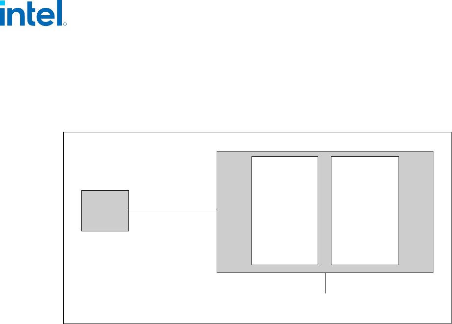
PCI Express* Configuration Mechanism
The PCI Express* (external graphics) link is mapped through a PCI-to-PCI bridge
structure.
Figure 27. PCI Express* Related Register Structures in the Processor
PCI-PCI Bridge
representing
root PCI
Express* ports
(Device 1)
PCI Compatible
Host Bridge
Device
(Device 0)
PCI
Express*
Device
PEG
DMI
The PCI Express* Host Bridge is required to translate the memory-mapped PCI
Express* configuration space accesses from the host processor to PCI Express*
configuration cycles. To maintain compatibility with PCI configuration addressing
mechanisms, it is recommended that system software access the enhanced
configuration space using 32-bit operations (32-bit aligned) only. Refer to the PCI
Express Base Specification for details of both the PCI-compatible and PCI Express*
Enhanced configuration mechanisms and transaction rules.
PCI Express* Equalization Methodology
Link equalization requires equalization for both TX and RX sides for the processor and
for the Endpoint device.
Adjusting transmitter and receiver of the lanes is done to improve signal reception
quality and for improving link robustness and electrical margin.
The link timing margins and voltage margins are strongly dependent on equalization of
the link.
The processor supports the following:
• Full TX Equalization: Three Taps Linear Equalization (Pre, Current and Post
cursors), with FS/LF (Full Swing /Low Frequency) values.
• Full RX Equalization and acquisition for AGC (Adaptive Gain Control), CDR (Clock
and Data Recovery), adaptive DFE (decision feedback equalizer) and adaptive
CTLE peaking (continuous time linear equalizer).
• Full adaptive phase 3 EQ compliant with PCI Express* Gen 3 and Gen 4
specification.
7.1.3
7.1.4
R
12th Generation Intel
®
Core
™
Processors—PCIe* Interface
12
th
Generation Intel
®
Core
™
Processors
Datasheet, Volume 1 of 2 February 2023
134 Doc. No.: 655258, Rev.: 010

PCI Express* Hot Plug
All PCIe* Root Ports support Express Card 1.0 based hot - plug that performs the
following:
• Presence Detect and Link Active Changed Support
• Interrupt Generation Support
• For hot plug support, refer to the below table
Port GEN S - Processor H - Processor P/U15 -
Processor
U9 -
Processor
PCIe010/011 GEN5 No No N/A N/A
PCIe060/062 GEN4 No No No No
Presence Detection
When a module is plugged in and power is supplied, the physical layer will detect the
presence of the device, and the root port sets SLSTS.PDS and SLSTS.PDC. If
SLCTL.PDE and SLCTL.HPE are both set, the root port will also generate an interrupt.
When a module is removed (using the physical layer detection), the root port clears
SLSTS.PDS and sets SLSTS.PDC. If SLCTL.PDE and SLCTL.HPE are both set, the root
port will also generate an interrupt.
SMI/SCI Generation
Interrupts for power - management events are not supported on legacy operating
systems. To support power - management on non - PCI Express* aware operating
systems, power management events can be routed to generate SCI. To generate SCI,
MPC.HPCE must be set. When set, enabled hot - plug events will cause SMSCS.HPCS
to be set.
Additionally, BIOS workaround for hot - plug can be supported by setting MPC.HPME.
When this bit is set, hot - plug events can cause SMI status bits in SMSCS to be set.
Supported hot - plug events and their corresponding SMSCS bit are:
• Presence Detect Changed – SMSCS.HPPDM
• Link Active State Changed – SMSCS.HPLAS
When any of these bits are set, SMI# will be generated. These bits are set regardless
of whether interrupts or SCI is enabled for hot - plug events. The SMI# may occur
concurrently with an interrupt or SCI.
NOTES
1. SMI is referred to Serial management Interfaces
2. SLSTS - Slot Status
3. SLCTL - Slot Control
4. For full register detail, refer to12
th
Generation Intel
®
Core
™
Processors Datasheet
Volume 2 (655259).
7.1.5
R
PCIe* Interface—12th Generation Intel
®
Core
™
Processors
12
th
Generation Intel
®
Core
™
Processors
February 2023 Datasheet, Volume 1 of 2
Doc. No.: 655258, Rev.: 010 135
8.0 Direct Media Interface and On Package Interface
Direct Media Interface (DMI)
NOTE
The DMI interface is only present in 2-Chip platform processors.
Direct Media Interface (DMI) connects the processor and the PCH.
The main characteristics are as follows:
• 8 lanes Gen 4 DMI support
• 4 lanes Gen 4 Reduced DMI support
• 16 GT/s point-to-point DMI interface to PCH
• DC coupling - no capacitors between the processor and the PCH
• PCH end-to-end lane reversal across the link
• L0 (Active) and L1 (Low power) states support
• Half-Swing support (low-power/low-voltage)
DMI Lane Reversal and Polarity Inversion
NOTE
Polarity Inversion and Lane Reversal on DMI Link are not allowed in S-Processor
segment. Lane reversal can only be allowed on the PCH side.
8.1
8.1.1
R
12th Generation Intel
®
Core
™
Processors—Direct Media Interface and On Package Interface
12
th
Generation Intel
®
Core
™
Processors
Datasheet, Volume 1 of 2 February 2023
136 Doc. No.: 655258, Rev.: 010
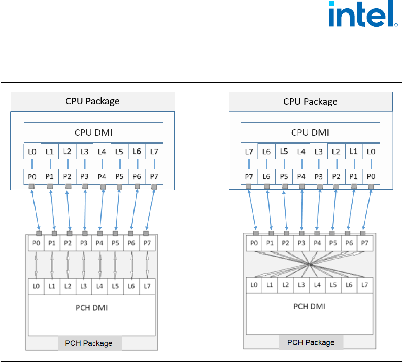
Figure 28. Example for DMI Lane Reversal Connection
1. DMI Lane Reversal is supported only on PCH-H and not on the Processor.
2. L[7:0] - Processor and PCH DMI Controller Logical Lane Numbers.
3. P[7:0] - Processor and PCH DMI Package Pin Lane Numbers.
DMI Error Flow
DMI can only generate SERR in response to errors; never SCI, SMI, MSI, PCI INT, or
GPE. Any DMI related SERR activity is associated with Device 0.
DMI Link Down
The DMI link going down is a fatal, unrecoverable error. If the DMI data link goes to
data link down, after the link was up, then the DMI link hangs the system by not
allowing the link to retrain to prevent data corruption. This link behavior is controlled
by the PCH.
Downstream transactions that had been successfully transmitted across the link prior
to the link going down may be processed as normal. No completions from
downstream, non-posted transactions are returned upstream over the DMI link after a
link down event.
On Package Interface (OPI)
8.1.2
8.1.3
8.2
R
Direct Media Interface and On Package Interface—12th Generation Intel
®
Core
™
Processors
12
th
Generation Intel
®
Core
™
Processors
February 2023 Datasheet, Volume 1 of 2
Doc. No.: 655258, Rev.: 010 137

OPI Support
The processor communicates with the PCIe using an internal interconnect BUS named
OPI.
Functional Description
OPI operates at 4 GT/s bus rate.
8.2.1
8.2.2
R
12th Generation Intel
®
Core
™
Processors—Direct Media Interface and On Package Interface
12
th
Generation Intel
®
Core
™
Processors
Datasheet, Volume 1 of 2 February 2023
138 Doc. No.: 655258, Rev.: 010

9.0 Graphics
Processor Graphics
The processor graphics is based on X
e
graphics core architecture that enables
substantial gains in performance and lower-power consumption over prior generations.
X
e
architecture supports up to 96 Execution Units (EUs) depending on the processor
SKU.
The processor graphics architecture delivers high dynamic range of scaling to address
segments spanning low power to high power, increased performance per watt, support
for next generation of APIs. X
e
scalable architecture is partitioned by usage domains
along Render/Geometry, Media, and Display. The architecture also delivers very low-
power video playback and next generation analytics and filters for imaging related
applications. The new Graphics Architecture includes 3D compute elements, Multi-
format HW assisted decode/encode pipeline, and Mid-Level Cache (MLC) for superior
high definition playback, video quality, and improved 3D performance and media.
Media Support (Intel
®
QuickSync and Clear Video Technology
HD)
X
e
implements multiple media video codecs in hardware as well as a rich set of image
processing algorithms.
NOTE
HEVC and VP9 support additional 10bpc, YCbCr 4:2:2 or 4:4:4 profiles. Refer
additional detail support matrix.
Hardware Accelerated Video Decode
X
e
implements a high-performance and low-power HW acceleration for video decoding
operations for multiple video codecs.
The HW decode is exposed by the graphics driver using the following APIs:
• Direct3D* 9 Video API (DXVA2)
• Direct3D11 Video API
• Direct3D12 Video API
• Intel Media SDK
• MFT (Media Foundation Transform) filters.
• Intel VA API
X
e
supports full HW accelerated video decoding for AVC/HEVC/VP9/JPEG/AV1.
9.1
9.1.1
9.1.1.1
R
Graphics—12th Generation Intel
®
Core
™
Processors
12
th
Generation Intel
®
Core
™
Processors
February 2023 Datasheet, Volume 1 of 2
Doc. No.: 655258, Rev.: 010 139

Table 58. Hardware Accelerated Video Decoding
Codec Profile Level Maximum Resolution
WMV9
Advanced
Main
Simple
L3
High
Simple
3840x3840
AVC/H264
High
Main
L5.2
4K
4:2:0 8bit 4K @ 60
JPEG/MJPEG Baseline Unified level 16K x16K
HEVC/H265
Main 12
Main 422 10
Main 422 12
Main 444
Main 444 10
Main 444 12
SCC main
SCC main 10
SCC main 444
SCC main 444 10
L6.1
5K @ 60
8K @ 60
VP9
1 (4:2:0 4:4:4 8 bit)
Unified level
4K @ 60
3 (4:2:0 4:4:4 10/12bit) 8K @ 60
AV1
0 (4:2:0 8-bit)
0 (4:2:0 10-bit)
L6.1
8K @ 60 (video)
16K x 16K (still picture)
NOTE
Video playback best performance can be achieved by enabling display MPO with
minimized EU workloads. In some test scenarios, it may act differently.
For example, 8k playback on less than 8k monitors, in non-full screen mode or some
UI operations and unexpected end user behaviors etc. - These will hit MPO limitation
or simply applications do not use MPO.
Then graphics driver need to use EU for rendering/composition, and 8K E2E playback
has dependency on EU counts capability.
Expected performance: More than 16 simultaneous decode streams @ 1080p.
NOTE
Actual performance depends on the processor SKU, content bit rate, and memory
frequency. Hardware decode for H264 SVC is not supported.
Hardware Accelerated Video Encode
Gen12 implements a low-power low-latency fixed function encoder and a high-quality
customizable encoder with hardware assisted motion estimation engine which
supports AVC, MPEG-2, HEVC, and VP9.
The HW encode is exposed by the graphics driver using the following APIs:
9.1.1.2
R
12th Generation Intel
®
Core
™
Processors—Graphics
12
th
Generation Intel
®
Core
™
Processors
Datasheet, Volume 1 of 2 February 2023
140 Doc. No.: 655258, Rev.: 010

• Intel
®
Media SDK
• MFT (Media Foundation Transform) filters
X
e
supports full HW accelerated video encoding for AVC/HEVC/VP9/JPEG.
Table 59. Hardware Accelerated Video Encode
Codec Profile Level Maximum Resolution
AVC/H264
High
Main
L5.1 2160p(4K)
JPEG Baseline — 16Kx16K
HEVC/H265
Main
Main10
Main 4:2:2 10
Main 4:4:4
Main 4:4:4 10
L5.1
4320p(8K)
16Kx4K @higher freq
VP9
0 (4:2:0 Chroma 8 bit)
1 (partial: 4:4:4 8 bit)
2 (partial: 4:2:0 10 bit)
3 (partial: 4:4:4 10 bit)
—
4320p(8K)
16Kx4K @higher freq
NOTE
Hardware encode for H264 SVC is not supported.
Hardware Accelerated Video Processing
There is hardware support for image processing functions such as De-interlacing, Film
cadence detection, Advanced Video Scaler (AVS), detail enhancement, gamut
compression, HD adaptive contrast enhancement, skin tone enhancement, total color
control, Chroma de-noise, SFC (Scalar and Format Conversion), memory compression,
Localized Adaptive Contrast Enhancement (LACE), spatial de-noise, Out-Of-Loop De-
blocking (from AVC decoder), 16 bpc support for de-noise/de-mosaic.
The HW video processing is exposed by the graphics driver using the following APIs:
• Direct3D* 9 Video API (DXVA2).
• Direct3D* 11 Video API.
• OneVPL
• MFT (Media Foundation Transform) filters.
• Intel
®
Graphics Control Library
• Intel VA API
NOTE
Not all features are supported by all the above APIs. Refer to the relevant
documentation for more details.
9.1.1.3
R
Graphics—12th Generation Intel
®
Core
™
Processors
12
th
Generation Intel
®
Core
™
Processors
February 2023 Datasheet, Volume 1 of 2
Doc. No.: 655258, Rev.: 010 141

Hardware Accelerated Transcoding
Transcoding is a combination of decode, video processing (optional) and encode. Using
the above hardware capabilities can accomplish a high-performance transcode
pipeline. There is not a dedicated API for transcoding.
The processor graphics supports the following transcoding features:
• High performance high quality flexible encoder for video editing, video archiving.
• Low-power low latency encoder for video conferencing, wireless display, and game
streaming.
• Lossless memory compression for media engine to reduce media power.
• High-quality Advanced Video Scaler (AVS)
• Low power Scaler and Format Converter.
Platform Graphics Hardware Feature
Hybrid Graphics
Microsoft* Windows* 10 operating system enables the Windows*10 Hybrid graphics
framework wherein the GPUs and their drivers can be simultaneously utilized to
provide users with the benefits of both performance capability of discrete GPU (dGPU)
and low-power display capability of the processor GPU (iGPU). For instance, when
there is a high-end 3D gaming workload in progress, the dGPU will process and render
the game frames using its graphics performance, while iGPU continues to perform the
display operations by compositing the frames rendered by dGPU. We recommend that
OEMS should seek further guidance from Microsoft* to confirm that the design fits all
the latest criteria defined by Microsoft* to support HG.
Microsoft* Hybrid Graphics definition includes the following:
1. The system contains a single integrated GPU and a single discrete GPU.
2. It is a design assumption that the discrete GPU has a significantly higher
performance than the integrated GPU.
3. Both GPUs shall be physically enclosed as part of the system.
a. Microsoft* Hybrid DOES NOT support hot-plugging of GPUs
b. OEMS should seek further guidance from Microsoft* before designing systems
with the concept of hot-plugging
4. Starting with Windows*10 Th1 (WDDM 2.0), a previous restriction that the
discrete GPU is a render-only device, with no displays connected to it, has been
removed. A render-only configuration with NO outputs is still allowed, just NOT
required.
9.1.1.4
9.2
9.2.1
R
12th Generation Intel
®
Core
™
Processors—Graphics
12
th
Generation Intel
®
Core
™
Processors
Datasheet, Volume 1 of 2 February 2023
142 Doc. No.: 655258, Rev.: 010
10.0 Display
Display Technologies Support
Technology Standard
eDP* 1.4b VESA* Embedded DisplayPort* Standard 1.4b
MIPI DSI
MIPI* DSI 2 Specification Version 1.0
MIPI* DPHY Specification Version 2.0
DisplayPort*
1.4a
VESA* DisplayPort* Standard 1.4a
VESA* DisplayPort* PHY Compliance Test Specification 1.4a
VESA* DisplayPort* Link Layer Compliance Test Specification 1.4
VESA* DisplayPort* Alt Mode on USB Type-C Standard Version 1.0b
HDMI* 2.1 High-Definition Multimedia Interface Specification Version 2.1
Notes: • Processor support native HDMI* 2.1 TMDS compatible ports
• Processor support non-native HDMI* 2.1 port by using DP*to HDMI* protocol converter.
Display Configuration
Table 60. Display Ports Availability and Link Rate for H/P/U - Processor Lines
Port S-Processor Line
H/P Processor
Line
4
U15 Processor
4
U9 Processor
4
DDI A
eDP* up to HBR3
DP* up to HBR3
1
HDMI* up to 5.94
Gbps
eDP* up to HBR3
MIPI DSI up to 2.5
Gbps
DP* up to HBR3
1
HDMI* up to 5.94
Gbps
eDP* up to HBR3
MIPI DSI up to 2.5
Gbps
DP* up to HBR3
1
HDMI* up to 5.94
Gbps
eDP* up to HBR3
MIPI DSI up to 2.5
Gbps
DP* up to HBR3
1
HDMI* up to 5.94
Gbps
DDI B
DP* up to HBR3
1
HDMI* up to 5.94
Gbps
eDP* up to HBR3
MIPI DSI up to 2.5
Gbps
DP* up to HBR3
1
HDMI* up to 5.94
Gbps
eDP* up to HBR3
MIPI DSI up to 2.5
Gbps
DP* up to HBR3
1
HDMI* up to 5.94
Gbps
eDP* up to HBR3
MIPI DSI up to 2.5
Gbps
DP* up to HBR3
1
HDMI* up to 5.94
Gbps
DDI C
DP* up to HBR3
1
HDMI* up to 5.94
Gbps
N/A N/A N/A
DDI D
DP* up to HBR3
1
HDMI* up to 5.94
Gbps
N/A N/A N/A
DDI E
DP* up to HBR3
1
HDMI* up to 5.94
Gbps
N/A N/A N/A
TCP 0 N/A DP* up to HBR3 DP* up to HBR3 DP* up to HBR3
continued...
10.1
10.2
R
Display—12th Generation Intel
®
Core
™
Processors
12
th
Generation Intel
®
Core
™
Processors
February 2023 Datasheet, Volume 1 of 2
Doc. No.: 655258, Rev.: 010 143

Port S-Processor Line
H/P Processor
Line
4
U15 Processor
4
U9 Processor
4
HDMI* up to 5.94
Gbps
HDMI* up to 5.94
Gbps
HDMI* up to 5.94
Gbps
TCP 1 N/A
DP* up to HBR3
HDMI* up to 5.94
Gbps
DP* up to HBR3
HDMI* up to 5.94
Gbps
DP* up to HBR3
HDMI* up to 5.94
Gbps
TCP 2 N/A
DP* up to HBR3
HDMI* up to 5.94
Gbps
DP* up to HBR3
HDMI* up to 5.94
Gbps
N/A
TCP 3 N/A
DP* up to HBR3
HDMI* up to 5.94
Gbps
DP* up to HBR3
HDMI* up to 5.94
Gbps
Notes: 1. On board re-timer is required.
2. HBR3 - 8.1 Gbps lane rate.
3. HBR2 - 5.4 Gbps lane rate.
4. Dual Embedded panels supported on P/H/U15 Processor lines using Port A and B
R
12th Generation Intel
®
Core
™
Processors—Display
12
th
Generation Intel
®
Core
™
Processors
Datasheet, Volume 1 of 2 February 2023
144 Doc. No.: 655258, Rev.: 010
Figure 29. S Processor Display Architecture
R
Display—12th Generation Intel
®
Core
™
Processors
12
th
Generation Intel
®
Core
™
Processors
February 2023 Datasheet, Volume 1 of 2
Doc. No.: 655258, Rev.: 010 145
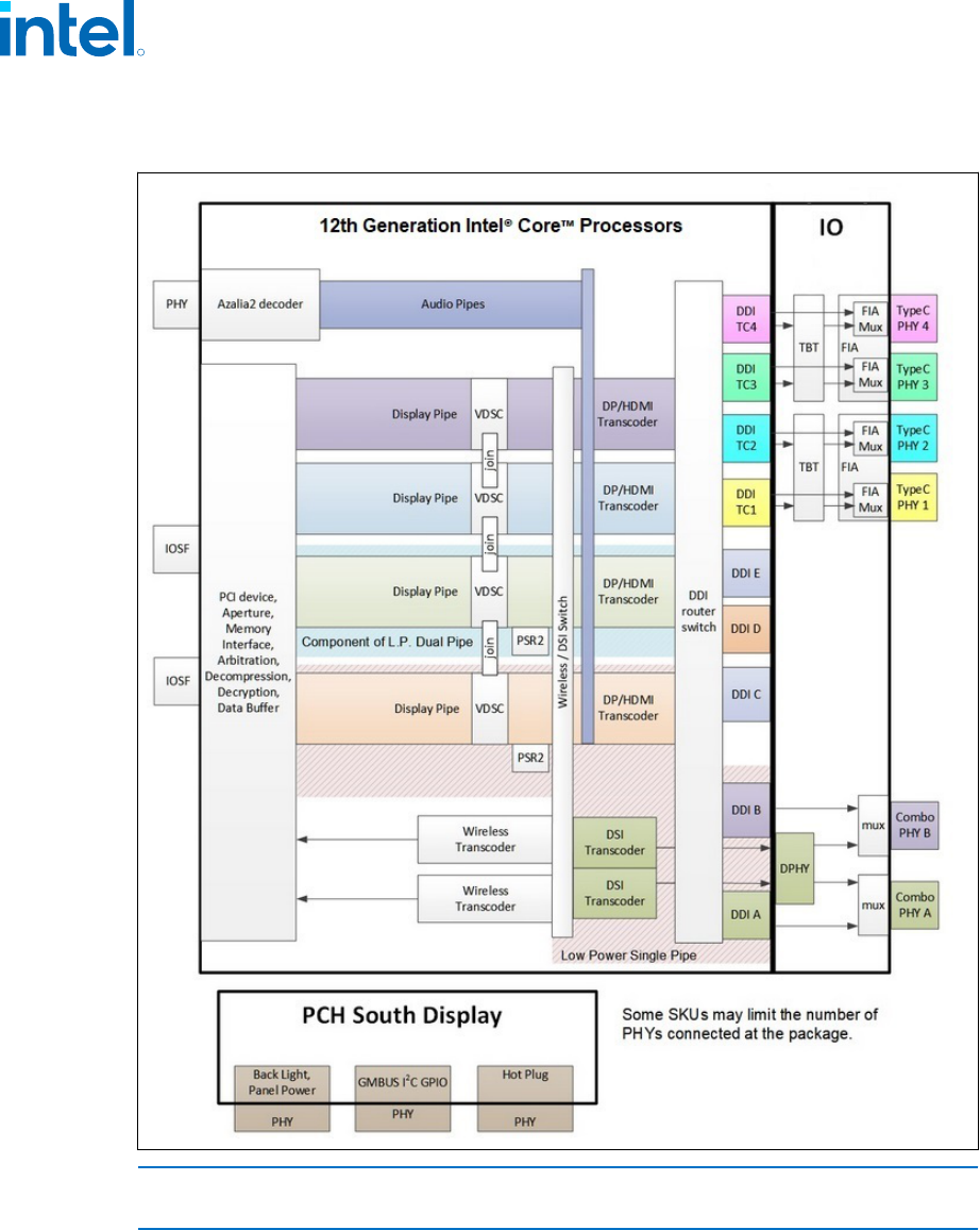
Figure 30. H/P/U Processor Display Architecture
NOTE
For port availability in the processor line, refer to the above table.
Display Features
General Capabilities
• Up to four simultaneous displays.
10.3
10.3.1
R
12th Generation Intel
®
Core
™
Processors—Display
12
th
Generation Intel
®
Core
™
Processors
Datasheet, Volume 1 of 2 February 2023
146 Doc. No.: 655258, Rev.: 010

— Single 8K60Hz panel, supported by joining two pipes over single port.
— Up to 4x4K60Hz display concurrent.
• Display interfaces supported:
— DDI interfaces supports DP*, HDMI*, DVI*, eDP*, DSI*
— TCP interfaces supports DP*, HDMI*, DVI*, Display Alt Mode over Type-C and
Display tunneled.
— Up to two wireless display captures.
• Audio stream support on external ports.
• HDR (High Dynamic Range) support.
• Four Display Pipes - Supporting blending, color adjustments, scaling and dithering.
• Transcoders - Containing the Timing generators supporting eDP*, DP*, HDMI*
interfaces.
• Up to two Low Power optimized pipes supporting Embedded DisplayPort* and/or
MIPI* DSI.
— LACE (Localized Adaptive Contrast Enhancement), supported up to 5 K
resolutions.
— 3D LUT - power efficient pixel modification function for color processing.
— FBC (Frame Buffer Compression) - power saving feature.
Multiple Display Configurations
The following multiple display configuration modes are supported (with appropriate
driver software):
• Single Display is a mode with one display port activated to display the output to
one display device.
• Display Clone is a mode with up to four display ports activated to drive the display
content of same color depth setting but potentially different refresh rate and
resolution settings to all the active display devices connected.
• Extended Desktop is a mode with up to four display ports activated to drive the
content with potentially different color depth, refresh rate, and resolution settings
on each of the active display devices connected.
High-bandwidth Digital Content Protection (HDCP)
HDCP is the technology for protecting high-definition content against unauthorized
copy or unreceptive between a source (computer, digital set top boxes, and so on) and
the sink (panels, monitor, and TVs). The processor supports both HDCP 2.3 and 1.4
content protection over wired displays (HDMI* and DisplayPort*).
The HDCP 1.4, 2.3 keys are integrated into the processor.
DisplayPort*
The DisplayPort* is a digital communication interface that uses differential signaling to
achieve a high-bandwidth bus interface designed to support connections between PCs
and monitors, projectors, and TV displays.
10.3.2
10.3.3
10.3.4
R
Display—12th Generation Intel
®
Core
™
Processors
12
th
Generation Intel
®
Core
™
Processors
February 2023 Datasheet, Volume 1 of 2
Doc. No.: 655258, Rev.: 010 147
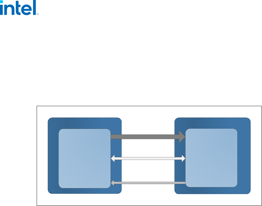
A DisplayPort* consists of a Main Link (four lanes), Auxiliary channel, and a Hot-Plug
Detect signal. The Main Link is a unidirectional, high-bandwidth, and low-latency
channel used for transport of isochronous data streams such as uncompressed video
and audio. The Auxiliary Channel (AUX CH) is a half-duplex bi-directional channel used
for link management and device control. The Hot-Plug Detect (HPD) signal serves as
an interrupt request from the sink device to the source device.
The processor is designed in accordance with VESA* DisplayPort* specification. Refer
to Display Technologies Support on page 143.
Figure 31. DisplayPort* Overview
Source Device Sink Device
Main Link
(Isochronous Streams)
AUX CH
(Link/Device Managemet)
Hot-Plug Detect
(Interrupt Request)
DisplayPort Tx
(Processor)
DisplayPort Rx
• Support main link of 1, 2, or 4 data lanes.
• Link rate support up to HBR3.
• Aux channel for Link/Device management.
• Hot Plug Detect.
• Support up to 36 BPP (Bit Per Pixel).
• Support SSC.
• Support YCbCR 4:4:4, YCbCR 4:2:0, YCbCR 4:2:2, and RGB color format.
• Support MST (Multi-Stream Transport).
• Support VESA DSC 1.1.
• Adaptive Sync.
Multi-Stream Transport (MST)
• The processor supports Multi-Stream Transport (MST), enabling multiple monitors
to be used via a single DisplayPort connector.
• Maximum MST DP supported resolution:
10.3.4.1
R
12th Generation Intel
®
Core
™
Processors—Display
12
th
Generation Intel
®
Core
™
Processors
Datasheet, Volume 1 of 2 February 2023
148 Doc. No.: 655258, Rev.: 010
Table 61. Display Resolutions and Link Bandwidth for Multi-Stream Transport
Calculations
Pixels per Line Lines
Refresh Rate
[Hz]
Pixel Clock [MHz]
Link Bandwidth
[Gbps]
1920 1080 60 148.5 4.46
1920 1200 60 154 4.62
2048 1152 60 156.75 4.70
2048 1280 60 174.25 5.23
2048 1536 60 209.25 6.28
2304 1440 60 218.75 6.56
2560 1440 60 241.5 7.25
3840 2160 30 262.75 7.88
2560 1600 60 268.5 8.06
2880 1800 60 337.5 10.13
3200 2400 60 497.75 14.93
3840 2160 60 533.25 16.00
4096 2160 60 556.75 16.70
4096 2304 60 605 18.15
5120 3200 60 1042.5 31.28
Notes: 1. All the above is related to bit depth of 24.
2. The data rate for a given video mode can be calculated as- Data Rate = Pixel Frequency * Bit
Depth.
3. The bandwidth requirements for a given video mode can be calculated as: Bandwidth = Data
Rate * 1.25 (for 8b/10b coding overhead).
4. The link bandwidth depends if the standards is reduced blanking or not.
If the standard is not reduced blanking - the expected bandwidth may be higher.
For more details, refer to VESA and Industry Standards and Guidelines for Computer Display
Monitor Timing (DMT). Version 1.0, Rev. 13 February 8, 2013
5. To calculate what are the resolutions that can be supported in MST configurations, follow the
below guidelines:
a. Identify what is the link bandwidth column according to the requested display resolution.
b. Summarize the bandwidth for two of three displays accordingly, and make sure the final
result is below 21.6 Gbps. (for example: 4 lanes HBR2 bit rate)
For example:
a. Docking two displays: 3840x2160@60 Hz + 1920x1200@60hz = 16 + 4.62 = 20.62 Gbps
[Supported]
b. Docking three displays: 3840x2160@30 Hz + 3840x2160@30 Hz + 1920x1080@60 Hz =
7.88 + 7.88 + 4.16 = 19.92 Gbps [Supported].
Table 62. DisplayPort Maximum Resolution
Standard
S-Processor
Line
H/P-Processor Line U-Processor Line
DP* 4096x2304 60
Hz 36 bpp
5120x3200 60
Hz 24 bpp
4096x2304 60Hz 36bpp
5120x3200 60Hz 24bpp
4096x2304 60Hz
36bpp
5120x3200 60Hz
24bpp
DP* with DSC
4
5120x3200
120 Hz 30 bpp
5120x3200 120Hz 30bpp
5120x3200 120Hz
30bpp
continued...
R
Display—12th Generation Intel
®
Core
™
Processors
12
th
Generation Intel
®
Core
™
Processors
February 2023 Datasheet, Volume 1 of 2
Doc. No.: 655258, Rev.: 010 149

Standard
S-Processor
Line
H/P-Processor Line U-Processor Line
7680x4320 60
Hz 30 bpp
7680x4320 60Hz 30bpp
7680x4320 60Hz
30bpp
Notes: 1. Maximum resolution is based on the implementation of 4 lanes at HBR3 link data rate.
2. bpp - bit per pixel.
3. Resolution support is subject to memory BW availability.
4. Resolutions will consume two display pipes.
High-Definition Multimedia Interface (HDMI*)
The High-Definition Multimedia Interface (HDMI*) is provided for transmitting
uncompressed digital audio and video signals from DVD players, set-top boxes, and
other audio-visual sources to television sets, projectors, and other video displays. It
can carry high-quality multi-channel audio data and all standard and high-definition
consumer electronics video formats. The HDMI display interface connecting the
processor and display devices uses transition minimized differential signaling (TMDS)
to carry audiovisual information through the same HDMI cable.
HDMI* includes three separate communications channels: TMDS, DDC, and the
optional CEC (consumer electronics control). CEC is not supported on the processor.
As shown in the following figure, the HDMI* cable carries four differential pairs that
make up the TMDS data and clock channels. These channels are used to carry video,
audio, and auxiliary data. In addition, HDMI carries a VESA DDC. The DDC is used by
an HDMI* Source to determine the capabilities and characteristics of the Sink.
Audio, video, and auxiliary (control/status) data is transmitted across the three TMDS
data channels. The video pixel clock is transmitted on the TMDS clock channel and is
used by the receiver for data recovery on the three data channels. The digital display
data signals driven natively through the PCH are AC coupled and needs level shifting
to convert the AC coupled signals to the HDMI* compliant digital signals. The
processor HDMI* interface is designed in accordance with the High-Definition
Multimedia Interface.
10.3.5
R
12th Generation Intel
®
Core
™
Processors—Display
12
th
Generation Intel
®
Core
™
Processors
Datasheet, Volume 1 of 2 February 2023
150 Doc. No.: 655258, Rev.: 010
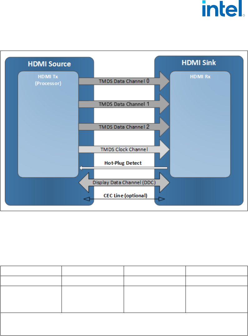
Figure 32. HDMI* Overview
• DDC (Display Data Channel) channel.
• Support YCbCR 4:4:4, YCbCR 4:2:0, YCbCR 4:2:2, and RGB color format.
• Support up to 36 BPP (Bit Per Pixel).
• Hot Plug Detect.
Table 63. HDMI Maximum Resolution
Standard S-Processor Line H/P-Processor Line U-Processor Line
HDMI 1.4 4Kx2K 24-30 Hz 24 bpp 4Kx2K 24-30 Hz 24bpp 4Kx2K 24-30 Hz 24bpp
HDMI 2.1 TMDS
Compatible
4Kx2K 48-60 Hz 24 bpp
(RGB/YUV444)
4Kx2K 48-60 Hz 12 bpc
(YUV420)
4Kx2K 48-60Hz 24bpp
(RGB/YUV444)
4Kx2K 48-60Hz 12bpc
(YUV420)
4Kx2K 48-60Hz 24bpp
(RGB/YUV444)
4Kx2K 48-60Hz 12bpc
(YUV420)
Notes: 1. bpp - bit per pixel.
2. Resolution support is subject to memory BW availability.
3. HDMI2.1 can be supported using PCON (DP1.4 to HDMI2.1 protocol converter).
embedded DisplayPort* (eDP*)
The embedded DisplayPort* (eDP*) is an embedded version of the DisplayPort
standard oriented towards applications such as notebook and All-In-One PCs. Like
DisplayPort, embedded DisplayPort* also consists of the Main Link, Auxiliary channel,
and an optional Hot-Plug Detect signal.
• Supported on Low power optimized pipes.
• Support up to HBR3 link rate.
• Support Backlight PWM control and enable signals, and power enable.
10.3.6
R
Display—12th Generation Intel
®
Core
™
Processors
12
th
Generation Intel
®
Core
™
Processors
February 2023 Datasheet, Volume 1 of 2
Doc. No.: 655258, Rev.: 010 151
• Support VESA DSC 1.1.
• Support SSC.
• Panel Self Refresh 1.
• Panel Self Refresh 2 (supported on P/H/U processor lines).
• MSO 2x2 (Multi Segment Operation).
• Dedicated Aux channel.
• Adaptive Sync.
Table 64. Embedded DisplayPort Maximum Resolution
Standard S/HX-Processor Line
1
H/P-Processor Line U-Processor Line
eDP* 4096x2304 60 Hz 36 bpp
5120x3200 60 Hz 24 bpp
4096x2304 60Hz 36bpp
5120x3200 60Hz 24bpp
4096x2304 60Hz 36bpp
5120x3200 60Hz 24bpp
eDP* with DSC
5
5120x3200 120 Hz 30
bpp
5120x3200 120Hz 30bpp 5120x3200 120Hz 30bpp
Notes: 1. Maximum resolution is based on the implementation of 4 lanes at HBR3 link data rate.
2. PSR2 supported for H/P/U processor lines only and up to 5 K resolutions.
3. bpp - bit per pixel.
4. Resolution support is subject to memory BW availability.
5. High resolution panels supporting Display Stream Compression (DSC) are supported,
technology enablement may be limited due to low market availability.
MIPI* DSI
Display Serial Interface (DSI*) specifies the interface between a host processor and
peripherals such as a display module. DSI is a high speed and high performance serial
interface that offers efficient and low power connectivity between the processor and
the display module.
• One link x8 data lanes or two links each with x4 lanes support.
• Supported on Low power optimized pipes.
• Support Backlight PWM control and enable signals, and power enable.
• Support VESA DSC (Data Stream Compression).
10.3.7
R
12th Generation Intel
®
Core
™
Processors—Display
12
th
Generation Intel
®
Core
™
Processors
Datasheet, Volume 1 of 2 February 2023
152 Doc. No.: 655258, Rev.: 010
Figure 33. MIPI* DSI Overview
Source Device Sink Device
Data Lane n
Data Lane 0
High Speed Clock
Host Device
(Processor)
Display
Table 65. MIPI* DSI Maximum Resolution
Standard S-Processor Line H/P-Processor Line U-Processor Line
MIPI* DSI (Single
Link)
N/A 3200x2000 @60 Hz 24
bpp
3200x2000 @60 Hz 24 bpp
MIPI* DSI (Single
Link) with DSC
N/A 5120x3200 @60 Hz 24
bpp
5120x3200 @60 Hz 24 bpp
MIPI* DSI (Dual Link) N/A 4096x2304 @60 Hz 24
bpp
3840x2160 @60 Hz 24
bpp
4096x2304 @60 Hz 24 bpp
3840x2160 @60 Hz 24 bpp
MIPI* DSI (Dual Link)
with DSC
N/A 5120x3200 @60 Hz 24
bpp
5120x3200 @60 Hz 24 bpp
Notes: 1. MIPI DSI is available on H/P/U Processor Lines only.
2. bpp - bit per pixel.
3. Resolution support is subject to memory BW availability.
Integrated Audio
• HDMI* and DisplayPort interfaces can carry audio along with video.
• The processor supports three High Definition audio streams on four digital ports
simultaneously (the DMA controllers are in PCH).
• The integrated audio processing (DSP) is performed by the PCH and delivered to
the processor using the AUDIO_SDI and AUDIO_CLK inputs pins.
• The AUDIO_SDO output pin is used to carry responses back to the PCH.
• Supports only the internal HDMI and DP CODECs.
Table 66. Processor Supported Audio Formats over HDMI* and DisplayPort*
Audio Formats HDMI* DisplayPort*
AC-3 Dolby* Digital Yes Yes
Dolby* Digital Plus Yes Yes
continued...
10.3.8
R
Display—12th Generation Intel
®
Core
™
Processors
12
th
Generation Intel
®
Core
™
Processors
February 2023 Datasheet, Volume 1 of 2
Doc. No.: 655258, Rev.: 010 153
Audio Formats HDMI* DisplayPort*
DTS-HD* Yes Yes
LPCM, 192 kHz/24 bit, 6 Channel Yes Yes
Dolby* TrueHD, DTS-HD Master Audio*
(Lossless Blu-Ray Disc* Audio Format)
Yes Yes
The processor will continue to support Silent stream. A Silent stream is an integrated
audio feature that enables short audio streams, such as system events to be heard
over the HDMI* and DisplayPort* monitors. The processor supports silent streams
over the HDMI and DisplayPort interfaces at 44.1 kHz, 48 kHz, 88.2 kHz, 96 kHz,
176.4 kHz, and 192 kHz sampling rates and silent multi-stream support.
R
12th Generation Intel
®
Core
™
Processors—Display
12
th
Generation Intel
®
Core
™
Processors
Datasheet, Volume 1 of 2 February 2023
154 Doc. No.: 655258, Rev.: 010

11.0 Camera/MIPI
Camer/MIPI is supported on the following processor line.
• P-Processor line
• H-Processor line
• U-Processor line
NOTE
The availability of the features above may vary between different processor SKUs.
Camera Pipe Support
The IPU6se fixed function pipe supports the following functions:
• Black level correction;
• White balance;
• Color matching;
• Lens shading (vignette) correction;
• Color crosstalk (color shading) correction;
• Dynamic defect pixel replacement;
• Auto-focus-pixel (PDAF) hiding;
• High quality demosaic;
• Scaling and format conversion;
• Temporal noise reduction running on Intel graphics.
MIPI* CSI-2 Camera Interconnect
The Camera I/O Controller provides a native/integrated interconnect to camera
sensors, compliant with MIPI* CSI-2 V2.0 protocol. Total of 8 data+4 clock lanes are
available for the camera interface supporting up to 4 sensors .
Data transmission interface (referred as CSI-2) is a unidirectional differential serial
interface with data and clock signals; the physical layer of this interface is the MIPI*
Alliance Specification for D-PHY.
The control interface (referred as CCI) is a bi-directional control interface compatible
with I
2
C standard.
11.1
11.2
R
Camera/MIPI—12th Generation Intel
®
Core
™
Processors
12
th
Generation Intel
®
Core
™
Processors
February 2023 Datasheet, Volume 1 of 2
Doc. No.: 655258, Rev.: 010 155
Camera Control Logic
The camera infrastructure supports several architectural options for camera control
utilizing camera PMIC and/or discrete logic. IPU6 control options utilize I
2
C for
bidirectional communication and PCH GPIOs to drive various control functions.
Camera Modules
Intel maintains an Intel User Facing Camera Approved Vendor List and Intel World-
Facing Approved Vendor List to simplify system design. Additional services are
available to support non-AVL options.
CSI-2 Lane Configuration
Table 67. CSI-2 Lane Configuration for H/P/U-Processor Lines
Port Data/Clock Configuration Option 1 Configuration Option 2
Port A Clock NA
x2
Port A Lane 0
x4
Port A Lane 1
Port B Clock
x2
Port B Lane 0
Port B Lane 1
Port C Clock
x4
x2Port C Lane 0
Port C Lane 1
Port D Lane 0
x2
Port D Lane 1
Port D Clock NA
11.2.1
11.2.2
11.2.3
R
12th Generation Intel
®
Core
™
Processors—Camera/MIPI
12
th
Generation Intel
®
Core
™
Processors
Datasheet, Volume 1 of 2 February 2023
156 Doc. No.: 655258, Rev.: 010
12.0 Signal Description
This chapter describes the processor signals. They are arranged in functional groups
according to their associated interface or category. The notations in the following table
are used to describe the signal type.
The signal description also includes the type of buffer used for the particular signal
(refer to the following table).
Table 68. Signal Tables Terminology
Notation Signal Type
I Input pin
O Output pin
I/O Input/Output, Bi-directional pin
SE Single Ended Link
Diff Differential Link
CMOS CMOS buffers. 1.05 V- tolerant
OD Open Drain buffer
LPDDR4x LPDDR4x buffers: 1.1 V-tolerant
LPDDR5 LPDDR5 buffers
DDR4 DDR4 buffers: 1.2 V-tolerant
DDR5 DDR5 buffers: 1.1 V-tolerant
A
Analog reference or output. May be used as a threshold voltage or for buffer
compensation
GTL Gunning Transceiver Logic signaling technology
Ref Voltage Reference signal
Availability Signal Availability condition - based on segment, SKU, platform type or any other factor
Asynchronous 1 Signal has no timing relationship with any reference clock.
Note: Qualifier for a buffer type.
R
Signal Description—12th Generation Intel
®
Core
™
Processors
12
th
Generation Intel
®
Core
™
Processors
February 2023 Datasheet, Volume 1 of 2
Doc. No.: 655258, Rev.: 010 157

System Memory Interface
DDR4 Memory Interface
Table 69. DDR4 Memory Interface
Signal Name Description Dir.
Buffer
Type
Link
Type
Availability
DDR0_DQ0[7:0]
DDR0_DQ1[7:0]
DDR0_DQ2[7:0]
DDR0_DQ3[7:0]
DDR0_DQ4[7:0]
DDR0_DQ5[7:0]
DDR0_DQ6[7:0]
DDR0_DQ7[7:0]
DDR0_DQ8[7:0]
DDR1_DQ0[7:0]
DDR1_DQ1[7:0]
DDR1_DQ2[7:0]
DDR1_DQ3[7:0]
DDR1_DQ4[7:0]
DDR1_DQ5[7:0]
DDR1_DQ6[7:0]
DDR1_DQ7[7:0]
DDR1_DQ8[7:0]
Data Buses: Data
signals interface to the
SDRAM data buses.
Example:
DDR0_DQ2[5] refers to
DDR channel 0, Byte 2,
Bit 5.
I/O DDR4 SE
S Processor
Line
P Processor
Line
H Processor
Line
U15
Processor
DDR0_DQSP[8:0]
DDR1_DQSP[8:0]
DDR0_DQSN[8:0]
DDR1_DQSN[8:0]
Data Strobes:
Differential data strobe
pairs. The data is
captured at the crossing
point of DQS during
reading and write
transactions.
Example: DDR0_DQSP0
refers to DQSP of DDR
channel 0, Byte 0.
I/O DDR4 Diff
S Processor
Line
P Processor
Line
H Processor
Line
U15
Processor
DDR0_CLKN[3:0]
DDR0_CLKP[3:0]
DDR1_CLKN[3:0]
DDR1_CLKP[3:0]
SDRAM Differential
Clock: Differential
clocks signal pairs, pair
per rank. The crossing
of the positive edge and
the negative edge of
their complement are
used to sample the
command and control
signals on the SDRAM.
O DDR4 Diff
S Processor
Line
DDR0_CLK_N[1:0]
DDR0_CLK_P[1:0]
DDR1_CLK_N[1:0]
DDR1_CLK_P[1:0]
SDRAM Differential
Clock: Differential
clocks signal pairs, pair
per rank. The crossing
of the positive edge and
the negative edge of
their complement are
used to sample the
command and control
signals on the SDRAM.
O DDR4 Diff
P Processor
Line
H Processor
Line
U15
Processor
DDR0_CKE[3:0]
DDR1_CKE[3:0]
Clock Enable: (1 per
rank). These signals are
used to:
O DDR4 SE
S Processor
Line
continued...
12.1
12.1.1
R
12th Generation Intel
®
Core
™
Processors—Signal Description
12
th
Generation Intel
®
Core
™
Processors
Datasheet, Volume 1 of 2 February 2023
158 Doc. No.: 655258, Rev.: 010

Signal Name Description Dir.
Buffer
Type
Link
Type
Availability
• Initialize the SDRAMs
during power-up.
• Power-down SDRAM
ranks.
• Place all SDRAM
ranks into and out of
self-refresh during
STR (Suspend to
RAM).
P Processor
Line
H Processor
Line
U15
Processor
DDR0_CS[3:0]
DDR1_CS[3:0]
Chip Select: (1 per
rank). These signals are
used to select particular
SDRAM components
during the active state.
There is one Chip Select
for each SDRAM rank.
O DDR4 SE
S Processor
Line
P Processor
Line
H Processor
Line
U15
Processor
DDR0_ODT[3:0]
DDR1_ODT[3:0]
On Die Termination:
(1 per rank). Active
SDRAM Termination
Control.
O DDR4 SE
S Processor
Line
P Processor
Line
H Processor
Line
U15
Processor
DDR0_MA[16:0]
DDR1_MA[16:0]
Address: These signals
are used to provide the
multiplexed row and
column address to the
SDRAM.
DDR0_MA[16] uses as
RAS# signal
DDR0_MA[15] uses as
CAS# signal
DDR0_MA[14] uses as
WE# signal
DDR1_MA[16] uses as
RAS# signal
DDR1_MA[15] uses as
CAS# signal
DDR1_MA[14] uses as
WE# signal
O DDR4 SE
S Processor
Line
P Processor
Line
H Processor
Line
U15
Processor
DDR0_ACT#
DDR1_ACT#
Activation Command:
ACT# HIGH along with
CS_N determines that
the signals addresses
below have command
functionality.
O DDR4 SE
S Processor
Line
P Processor
Line
H Processor
Line
U15
Processor
DDR0_BG[1:0]
DDR1_BG[1:0]
Bank Group: BG[1:0]
define to which bank
group an Active,
reading, Write or
Precharge command is
being applied.
O DDR4 SE
S Processor
Line
P Processor
Line
H Processor
Line
continued...
R
Signal Description—12th Generation Intel
®
Core
™
Processors
12
th
Generation Intel
®
Core
™
Processors
February 2023 Datasheet, Volume 1 of 2
Doc. No.: 655258, Rev.: 010 159
Signal Name Description Dir.
Buffer
Type
Link
Type
Availability
BG0 also determines
which mode register is
to be accessed during a
MRS cycle.
U15
Processor
DDR0_BA[1:0]
DDR1_BA[1:0]
Bank Address: BA[1:0]
define to which bank an
Active, reading, Write or
Precharge command is
being applied. Bank
address also determines
which mode register is
to be accessed during a
MRS cycle.
O DDR4 SE
S Processor
Line
P Processor
Line
H Processor
Line
U15
Processor
DDR0_PAR
DDR1_PAR
Command and
Address Parity: These
signals are used for
parity check.
O A SE
S Processor
Line
P Processor
Line
H Processor
Line
U15
Processor
DDR_VREF_CA[3:0]
Memory Reference
Voltage for Command
and Address
O A SE
S Processor
Line
DDR0_VREF_CA0
DDR1_VREF_CA0
Memory Reference
Voltage for Command
and Address
O A SE
P Processor
Line
H Processor
Line
U15
Processor
DDR_VTT_CTL
System Memory
Power Gate Control:
When signal is high –
platform memory VTT
regulator is enable,
output high.
When signal is low -
Disables the platform
memory VTT regulator
in C8 and deeper and
S3.
O A SE
S Processor
Line
P Processor
Line
H Processor
Line
U15
Processor
DDR0_ALERT#
DDR1_ALERT#
Alert: This signal is
used at command
training only. It is
getting the Command
and Address Parity error
flag during training. CRC
feature is not supported.
I DDR4 SE
S Processor
Line
P Processor
Line
H Processor
Line
U15
Processor
LP4x-LP5 Memory Interface
Signal Name
Description Dir. Buffer Type Link Type Availability
DDR0_DQ[1:0][7:0]
DDR1_DQ[1:0][7:0]
Data Buses: Data
signals interface to the
SDRAM data buses.
I/O LP4x-LP5 SE P Processor Line
U Processor Line
continued...
12.1.2
R
12th Generation Intel
®
Core
™
Processors—Signal Description
12
th
Generation Intel
®
Core
™
Processors
Datasheet, Volume 1 of 2 February 2023
160 Doc. No.: 655258, Rev.: 010

Signal Name Description Dir. Buffer Type Link Type Availability
DDR2_DQ[1:0][7:0]
DDR3_DQ[1:0][7:0]
DDR4_DQ[1:0][7:0]
DDR5_DQ[1:0][7:0]
DDR6_DQ[1:0][7:0]
DDR7_DQ[1:0][7:0]
Example:
DDR0_DQ1[5] refers to
DDR channel 0, Byte 1,
Bit 5.
H Processor Line
DDR0_DQSP[1:0]
DDR1_DQSP[1:0]
DDR2_DQSP[1:0]
DDR3_DQSP[1:0]
DDR4_DQSP[1:0]
DDR5_DQSP[1:0]
DDR6_DQSP[1:0]
DDR7_DQSP[1:0]
DDR0_DQSN[1:0]
DDR1_DQSN[1:0]
DDR2_DQSN[1:0]
DDR3_DQSN[1:0]
DDR4_DQSN[1:0]
DDR5_DQSN[1:0]
DDR6_DQSN[1:0]
DDR7_DQSN[1:0]
Data Strobes:
Differential data strobe
pairs. The data is
captured at the crossing
point of DQS during
reading and write
transactions.
I/O LP4x-LP5 Diff P Processor Line
U Processor Line
H Processor Line
DDR0_CLK_N
DDR0_CLK_P
DDR1_CLK_N
DDR1_CLK_P
DDR2_CLK_N
DDR2_CLK_P
DDR3_CLK_N
DDR3_CLK_P
DDR4_CLK_N
DDR4_CLK_P
DDR5_CLK_N
DDR5_CLK_P
DDR6_CLK_N
DDR6_CLK_P
DDR7_CLK_N
DDR7_CLK_P
SDRAM Differential
Clock:
Differential clocks signal
pairs, pair per channel
and package. The
crossing of the positive
edge and the negative
edge of their
complement are used to
sample the command
and control signals on
the SDRAM.
O LP4x-LP5 Diff P Processor Line
U Processor Line
H Processor Line
DDR0_CKE[1:0]
DDR1_CKE[1:0]
DDR2_CKE[1:0]
DDR3_CKE[1:0]
DDR4_CKE[1:0]
DDR5_CKE[1:0]
DDR6_CKE[1:0]
DDR7_CKE[1:0]
Clock Enable: (1 per
rank) These signals are
used to:
• Initialize the SDRAMs
during power-up.
• Power-down SDRAM
ranks.
• Place all SDRAM
ranks into and out of
self-refresh during
STR.
O LP4x-LP5 SE P Processor Line
U Processor Line
H Processor Line
DDR0_CS[1:0]
DDR1_CS[1:0]
DDR2_CS[1:0]
DDR3_CS[1:0]
DDR4_CS[1:0]
Chip Select: (1 per
rank). These signals are
used to select particular
SDRAM components
O LP4x-LP5 SE P Processor Line
U Processor Line
H Processor Line
continued...
R
Signal Description—12th Generation Intel
®
Core
™
Processors
12
th
Generation Intel
®
Core
™
Processors
February 2023 Datasheet, Volume 1 of 2
Doc. No.: 655258, Rev.: 010 161
Signal Name Description Dir. Buffer Type Link Type Availability
DDR5_CS[1:0]
DDR6_CS[1:0]
DDR7_CS[1:0]
during the active state.
There is one Chip Select
for each SDRAM rank.
The Chip select signal is
Active High.
DDR0_CA[5:0]
DDR1_CA[5:0]
DDR2_CA[5:0]
DDR3_CA[5:0]
DDR4_CA[5:0]
DDR5_CA[5:0]
DDR6_CA[5:0]
DDR7_CA[5:0]
Command Address:
These signals are used
to provide the
multiplexed command
and address to the
SDRAM.
O LP4x-LP5 SE P Processor Line
U Processor Line
H Processor Line
DDR0_CA[6]
DDR1_CA[6]
DDR2_CA[6]
DDR3_CA[6]
DDR4_CA[6]
DDR5_CA[6]
DDR6_CA[6]
DDR7_CA[6]
Command Address:
These signals are used
to provide the
multiplexed command
and address to the
SDRAM.
O LP5 SE P Processor Line
U Processor Line
H Processor Line
DDR[7:0]_WCK_P
DDR[7:0]_WCK_N
Write Clocks: WCK_N
and WCK_P are
differential clocks used
for WRITE data capture
and READ data output.
O LP5 Diff P Processor Line
U Processor Line
H Processor Line
DDR_COMP
DDR_RCOMP
System Memory
Resistance
Compensation
A A SE P Processor Line
U Processor Line
H Processor Line
DRAM_RESET# Memory Reset O CMOS SE P Processor Line
U Processor Line
H Processor Line
DDR5 Memory Interface
Table 70. DDR5 Memory Interface
Signal Name Description Dir.
Buffer
Type
Link
Type
Availability
DDR0_DQ0[7:0]
DDR0_DQ1[7:0]
DDR0_DQ2[7:0]
DDR0_DQ3[7:0]
DDR0_DQ4[7:0]
DDR1_DQ0[7:0]
DDR1_DQ1[7:0]
DDR1_DQ2[7:0]
DDR1_DQ3[7:0]
DDR1_DQ4[7:0]
DDR2_DQ0[7:0]
DDR2_DQ1[7:0]
DDR2_DQ2[7:0]
Data Buses: Data signals interface
to the SDRAM data buses.
Example: DDR0_DQ2[5] refers to
DDR channel 0, Byte 2, Bit 5.
I/O DDR5 SE
S Processor Line
P Processor Line
continued...
12.1.3
R
12th Generation Intel
®
Core
™
Processors—Signal Description
12
th
Generation Intel
®
Core
™
Processors
Datasheet, Volume 1 of 2 February 2023
162 Doc. No.: 655258, Rev.: 010

Signal Name Description Dir.
Buffer
Type
Link
Type
Availability
DDR2_DQ3[7:0]
DDR2_DQ4[3:0]
DDR3_DQ0[7:0]
DDR3_DQ1[7:0]
DDR3_DQ2[7:0]
DDR3_DQ3[7:0]
DDR3_DQ4[3:0]
DDR0_DQSP[4:0]
DDR0_DQSN[4:0]
DDR1_DQSP[4:0]
DDR1_DQSN[4:0]
DDR2_DQSP[4:0]
DDR2_DQSN[4:0]
DDR3_DQSP[4:0]
DDR3_DQSN[4:0]
Data Strobes: Differential data
strobe pairs. The data is captured at
the crossing point of DQS during
reading and write transactions.
Example: DDR0_DQSP0 refers to
DQSP of DDR channel 0, Byte 0.
I/O DDR5 Diff
S Processor Line
P Processor Line
DDR0_CLKN[3:0]
DDR0_CLKP[3:0]
DDR1_CLKN[3:0]
DDR1_CLKP[3:0]
DDR2_CLKN[3:0]
DDR2_CLKP[3:0]
DDR3_CLKN[3:0]
DDR3_CLKP[3:0]
SDRAM Differential Clock:
Differential clocks signal pairs, pair
per rank. The crossing of the positive
edge and the negative edge of their
complement are used to sample the
command and control signals on the
SDRAM.
O DDR5 Diff S Processor Line
DDR0_CLK_N[1:0]
DDR0_CLK_P[1:0]
DDR1_CLK_N[1:0]
DDR1_CLK_P[1:0]
DDR2_CLK_N[1:0]
DDR2_CLK_P[1:0]
DDR3_CLK_N[1:0]
DDR3_CLK_P[1:0]
SDRAM Differential Clock:
Differential clocks signal pairs, pair
per rank. The crossing of the positive
edge and the negative edge of their
complement are used to sample the
command and control signals on the
SDRAM.
O DDR5 Diff P Processor Line
DDR0_CS[3:0]
DDR1_CS[3:0]
DDR2_CS[3:0]
DDR3_CS[3:0]
Chip Select: (1 per rank). These
signals are used to select particular
SDRAM components during the active
state. There is one Chip Select for
each SDRAM rank.
The Chip select signal is Active High.
O DDR5 SE
S Processor Line
P Processor Line
DDR0_CA[12:0]
DDR1_CA[12:0]
DDR2_CA[12:0]
DDR3_CA[12:0]
Command Address: These signals
are used to provide the multiplexed
command and address to the
SDRAM.
O DDR5 SE
S Processor Line
P Processor Line
DDR_VREF_CA[3:0]
Memory Reference Voltage for
Command and Address
O A SE S Processor Line
DDR0_ALERT#
DDR1_ALERT#
Alert: This signal is used at
command training only. It is getting
the Command and Address Parity
error flag during training. CRC
feature is not supported.
I DDR5 SE
S Processor Line
P Processor Line
R
Signal Description—12th Generation Intel
®
Core
™
Processors
12
th
Generation Intel
®
Core
™
Processors
February 2023 Datasheet, Volume 1 of 2
Doc. No.: 655258, Rev.: 010 163
PCI Express* Graphics (PEG) Signals
Signal Name Description Dir
Buffer
Type
Link
Type
Availability
PCIE_X4_TXP[[3:0]]
PCIE_X4_TXN[[3:0]]
PCIe Transmit Differential
Pairs
O PCIE* Diff S/HX Processor Line
PCIE_X4_RXP[[3:0]]
PCIE_X4_RXN[[3:0]]
PCIe Receive Differential
Pairs
I PCIE* Diff S/HX Processor Line
PCIE_X16_TXP[[15:0]]
PCIE_X16_TXN[[15:0]]
PCIe Transmit Differential
Pairs
O PCIE* Diff S/HX Processor Line
PCIE_X16_RXP[[15:0]]
PCIE_X16_RXN[[15:0]]
PCIe Receive Differential
Pairs
I PCIE* Diff S/HX Processor Line
PCIEX4_A_TX_P[[3:0]]
PCIEX4_A_TX_N[[3:0]]
PCIe Transmit Differential
Pairs
O PCIE* Diff
P Processor Line
U Processor Line
H Processor Line
PCIEX4_B_TXP[[3:0]]
PCIEX4_B_TXN[[3:0]]
PCIe Transmit Differential
Pairs
O PCIE* Diff P Processor Line
PCIEX4_A_RX_P[[3:0]]
PCIEX4_A_RX_N[[3:0]]
PCIe Receive Differential
Pairs
I PCIE* Diff
P Processor Line
U Processor Line
H Processor Line
PCIEX4_B_RXP[[3:0]]
PCIEX4_B_RXN[[3:0]]
PCIe Receive Differential
Pairs
I PCIE* Diff P Processor Line
PCIEX4_A_RCOMP_P
PCIEX4_A_RCOMP_N
Resistance Compensation
NA A Diff
P Processor Line
U Processor Line
H Processor Line
PCIEX4_A_RCOMP_P
PCIEX4_A_RCOMP_N
Resistance Compensation
NA A Diff U9 Processor Line
PCIEX4_B_RCOMP_P
PCIEX4_B_RCOMP_N
Resistance Compensation
NA A Diff
P Processor Line
H Processor Line
U15 Processor Line
PCIEX8_TX_P[[7:0]]
PCIEX8_TX_N[[7:0]]
PCIe Transmit Differential
Pairs
O PCIE* Diff H Processor Line
PCIEX8_RX_P[[7:0]]
PCIEX8_RX_N[[7:0]]
PCIe Receive Differential
Pairs
I PCIE* Diff H Processor Line
PCIEX8_RCOMP_P
PCIEX8_RCOMP_N
Resistance Compensation
NA A Diff H Processor Line
Direct Media Interface (DMI) Signals
Signal Name Description Dir
Buffer
Type
Link
Type
Availability
DMI_RXP[7:0]
DMI_RXN[7:0]
DMI Input from PCH: Direct
Media Interface receive
differential pairs.
I DMI Diff
S/HX-Processor Line
DMI_TXP[7:0]
DMI_TXN[7:0]
DMI Output from PCH: Direct
Media Interface transmit
differential pairs.
O DMI Diff
12.2
12.3
R
12th Generation Intel
®
Core
™
Processors—Signal Description
12
th
Generation Intel
®
Core
™
Processors
Datasheet, Volume 1 of 2 February 2023
164 Doc. No.: 655258, Rev.: 010
Reset and Miscellaneous Signals
Signal Name Description Dir.
Buffer
Type
Link
Type
Availability
EKEY
Socket Electronic Key
Used to distinguish between packages
with different pins assignment.
Connect this pin to the Enable signal of
the first VR in sequence. Or as
appropriate, to shut down complete
power to SOC/platform when a wrong
package is being used.
NA NA SE
S-Processor
Line
SKTOCC#
Socket Occupied: Pulled down directly
(0 Ohms) on the processor package to
the ground. There is no connection to
the processor silicon for this signal.
System board designers may use this
signal to determine if the processor is
present.
NA NA SE
S-Processor
Line
H-Processor
Line
P-Processor
Line
U-Processor
Line
CFG[17:0]
Configuration Signals: The CFG signals
have a default value of '1' if not
terminated on the board.
Intel recommends placing test points
on the board for CFG pins.
• CFG[1:0]: Reserved configuration
lane.
• CFG[2]: S-Processor Line
PCI Express* Static x16 Lanes
Numbering Reversal
• CFG[2]:
H-Processor Line
PCI Express* Static x8 Lanes
Numbering Reversal
• CFG[2]:
U9-Processor Line
Reserved
• CFG[3]: Reserved configuration
lane.
• CFG[4]: Reserved
• CFG[5]
S-Processor Line PCI
Express* Bifurcation
— 0 = 2 x8 PCI Express*
— 1 = 1 x16 PCI Express*
(default)
• CFG[5]
H/P/U15-Processor Line
Reserved configuration lanes.
• CFG[6]: Reserved configuration
lanes.
• CFG[7]: Reserved configuration
lanes.
• CFG[13:8]: Reserved configuration
lanes.
• CFG[14]:
S-Processor Line PEG60
Lane Reversal:
— 1 - (Default) Normal
— 0 - Reversed
• CFG[14]:
H/P/U15-Processor
Line PEG60 Lane Reversal:
— 1 - (Default) Normal
— 0 - Reversed
I/O GTL SE
S-Processor
Line
H-Processor
Line
P-Processor
Line
U-Processor
Line
continued...
12.4
R
Signal Description—12th Generation Intel
®
Core
™
Processors
12
th
Generation Intel
®
Core
™
Processors
February 2023 Datasheet, Volume 1 of 2
Doc. No.: 655258, Rev.: 010 165
Signal Name Description Dir.
Buffer
Type
Link
Type
Availability
• CFG[15]: H/P/U15-Processor
Line PEG62 Lane Reversal:
— 1 - (Default) Normal
— 0 - Reversed
• CFG[14]: U9 Processor Line
PEG60 Lane Reversal:
— 1 - (Default) Normal
— 0 - Reversed
• CFG[17:15]:
U9 and S-Processor
Line Reserved configuration lanes.
• CFG[17:16]:
H/P/U15-Processor
Line Reserved configuration lanes.
CFG_RCOMP Configuration Resistance Compensation NA NA SE
H-Processor
Line
P-Processor
Line
U-Processor
Line
VCC_CFG_PU_OUT
Power rail used by platform CFG straps
for pull up resistors.
O GTL SE
S-Processor
Line
H-Processor
Line
P-Processor
Line
EAR#
Stall reset sequence for early reset
phases debug until deasserted:
— 1 = (Default) Normal Operation; No
stall.
— 0 = Stall.
I CMOS SE
S-Processor
Line
H-Processor
Line
P-Processor
Line
U-Processor
Line
RESET#
Platform Reset pin driven by the PCH.
I CMOS SE
S-Processor
Line
CPU_ID
A PLATFORM indication signal, for
Compatibility option.
CMOS SE
S-Processor
Line
H-Processor
Line
P-Processor
Line
U-Processor
Line
PROC_TRIGIN Debug pin I CMOS SE
S-Processor
Line
PROC_TRIGOUT Debug pin O CMOS SE
S-Processor
Line
DRAM_RESET#
Memory Reset
O CMOS SE
H-Processor
Line
P-Processor
Line
U-Processor
Line
R
12th Generation Intel
®
Core
™
Processors—Signal Description
12
th
Generation Intel
®
Core
™
Processors
Datasheet, Volume 1 of 2 February 2023
166 Doc. No.: 655258, Rev.: 010
Display Interfaces
Digital Display Interface (DDI) Signals
Signal Name Description Dir.
Link
Type
Availability
DDIx_TXP[3:0]
DDIx_TXN[3:0]
Digital Display Interface Transmitter lanes.
DisplayPort, Embedded DisplayPort, HDMI and
MIPI DSI Differential Pairs.
O Diff
S Processor Line
P Processor Line
H Processor Line
U Processor Line
DDIx_AUXP
DDIx_AUXN
Digital Display Interface Display Port Auxiliary:
Half-duplex, bidirectional channel consist of
one differential pair for each channel.
MIPI DSI interface differential pair.
I/O Diff
DISP_UTILS_1
Digital Display Interface Utility Pin.
MIPI DSI Tearing effect signal
O
SE
DISP_UTILS_2
Digital Display Interface Utility Pin.
MIPI DSI Tearing effect signal.
O SE
DDIA_RCOMP
DDIB_RCOMP
DDI IO Compensation resistors.
U, P, Px, H processor lines only
A SE P Processor Line
H Processor Line
U Processor Line
Notes: • eDP*/DP*/HDMI*/DSI* implementation go along with additional sideband signals, for more information refer to
Intel
®
600 Series Chipset Family Platform Controller Hub Datasheet, Volume 1 of 2 (#648364).
• x Can be ports A, B, C, D, E
Digital Display Audio Signals
Signal Name
Description Dir. Link Type Availability
PROC_AUDOUT Serial Data Output for display audio interface O SE
S/HX Processor Line
PROC_AUDIN Serial Data Input for display audio interface I SE
PROC_AUDCLK Serial Data Clock I SE
USB Type-C Signals
Signal Name
Description Dir. Link
Type
Availability
TCP[1:0]_TX_P[1:0]
TCP[1:0]_TX_N[1:0]
TX Data Lane. O Diff P Processor Line
H Processor Line
U Processor Line
TCP[3:2]_TX_P[1:0]
TCP[3:2]_TX_N[1:0]
TX Data Lane. O Diff P Processor Line
H Processor Line
U15 Processor Line
TCP[1:0]_TXRX_P[1:0]
TCP[1:0]_TXRX_N[1:0]
RX Data Lane, also serves as
the secondary TX data lane.
I/O Diff P Processor Line
H Processor Line
U Processor Line
TCP[3:2]_TXRX_P[1:0]
TCP[3:2]_TXRX_N[1:0]
RX Data Lane, also serves as
the secondary TX data lane.
I/O Diff P Processor Line
H Processor Line
U15 Processor Line
continued...
12.5
12.5.1
12.5.2
12.6
R
Signal Description—12th Generation Intel
®
Core
™
Processors
12
th
Generation Intel
®
Core
™
Processors
February 2023 Datasheet, Volume 1 of 2
Doc. No.: 655258, Rev.: 010 167

Signal Name Description Dir. Link
Type
Availability
TCP[1:0]_AUX_P
TCP[1:0]_AUX_N
Common Lane AUX-PAD. I/O Diff P Processor Line
H Processor Line
U Processor Line
TCP[3:2]_AUX_P
TCP[3:2]_AUX_N
Common Lane AUX-PAD. I/O Diff P Processor Line
H Processor Line
U15 Processor Line
TCP0_RCOMP
TCP_RCOMP
Type-C Resistance
Compensation.
N/A Diff P Processor Line
H Processor Line
U Processor Line
MIPI* CSI-2 Interface Signals
Signal Name Description Dir. Buffer Type Link Type Availability
CSI_A_DP[1:0]
CSI_A_DN[1:0]
CSI-2 Ports Data lane I DPHY Diff
P Processor Line
H Processor
Line
U Processor Line
CSI_D_DP[1:0]
CSI_D_DN[1:0]
CSI-2 Ports Data lane I DPHY Diff
P Processor Line
H Processor
Line
U Processor Line
CSI_B_DP[3:0]
CSI_B_DN[3:0]
CSI-2 Ports Data lane I DPHY Diff
P Processor Line
H Processor
Line
U Processor Line
CSI_C_DP[3:0]
CSI_C_DN[3:0]
CSI-2 Ports Data lane I DPHY Diff
P Processor Line
H Processor
Line
U Processor Line
CSI_A_CLK_P
CSI_A_CLK_N
CSI 2 Port A Clock
lane
I DPHY Diff
P Processor Line
H Processor
Line
U Processor Line
CSI_B_CLK_P
CSI_B_CLK_N
CSI 2 Port A Clock
lane
I DPHY Diff
P Processor Line
H Processor
Line
U Processor Line
CSI_C_CLK_P
CSI_C_CLK_N
CSI 2 Port A Clock
lane
I DPHY Diff
P Processor Line
H Processor
Line
U Processor Line
CSI_D_CLK_P
CSI_D_CLK_N
CSI 2 Port A Clock
lane
I DPHY Diff
P Processor Line
H Processor
Line
U Processor Line
CSI_RCOMP
CSI Resistance
Compensation
N/A N/A SE
P Processor Line
H Processor
Line
U Processor Line
12.7
R
12th Generation Intel
®
Core
™
Processors—Signal Description
12
th
Generation Intel
®
Core
™
Processors
Datasheet, Volume 1 of 2 February 2023
168 Doc. No.: 655258, Rev.: 010
Processor Clocking Signals
Signal Name Description
Dir
.
Buffer
Type
Link
Type
Availability
BCLK_P
BCLK_N
100 MHz Differential bus clock input to the
processor.
I Diff
S-Processor Line
CLK_NSSC_P
CLK_NSSC_N
38.4 MHz Differential bus clock input to the
processor.
I Diff
PCI_BCLKP
PCI_BCLKN
100 MHz Clock for PCI Express* logic
I Diff
Testability Signals
Signal Name Description Dir.
Buffer
Type
Link
Type
Availability
BPM#[3:0]
Breakpoint and Performance Monitor
Signals: Outputs from the processor that
indicate the status of breakpoints and
programmable counters used for monitoring
processor performance.
I/O GTL SE
S Processor Line
P Processor Line
H Processor Line
U Processor Line
PROC_PRDY#
Probe Mode Ready: PROC_PRDY# is a
processor output used by debug tools to
determine processor debug readiness.
O OD SE
S Processor Line
P Processor Line
H Processor Line
U Processor Line
PROC_PREQ#
Probe Mode Request: PROC_PREQ# is used by
debug tools to request debug operation of the
processor.
I GTL SE
S Processor Line
P Processor Line
H Processor Line
U Processor Line
PROC_TCK
Test Clock: This signal provides the clock input
for the processor Test Bus (also known as the
Test Access Port). This signal should be driven
low or allowed to float during power on Reset.
I GTL SE S Processor Line
PROC_TDI
Test Data In: This signal transfers serial test
data into the processor. This signal provides the
serial input needed for JTAG specification
support.
I GTL SE S Processor Line
PROC_TDO
Test Data Out: This signal transfers serial test
data out of the processor. This signal provides
the serial output needed for JTAG specification
support.
O OD SE S Processor Line
PROC_TMS
Test Mode Select: A JTAG specification support
signal used by debug tools.
I GTL SE S Processor Line
PROC_JTAG_TCK
Test Clock: This signal provides the clock input
for the processor Test Bus (also known as the
Test Access Port). This signal should be driven
low or allowed to float during power on Reset.
I GTL SE
P Processor Line
H Processor Line
U Processor Line
PROC_JTAG_TDI
Test Data In: This signal transfers serial test
data into the processor. This signal provides the
serial input needed for JTAG specification
support.
I GTL SE
P Processor Line
H Processor Line
U Processor Line
continued...
12.8
12.9
R
Signal Description—12th Generation Intel
®
Core
™
Processors
12
th
Generation Intel
®
Core
™
Processors
February 2023 Datasheet, Volume 1 of 2
Doc. No.: 655258, Rev.: 010 169

Signal Name Description Dir.
Buffer
Type
Link
Type
Availability
PROC_JTAG_TDO
Test Data Out: This signal transfers serial test
data out of the processor. This signal provides
the serial output needed for JTAG specification
support.
O OD SE
P Processor Line
H Processor Line
U Processor Line
PROC_JTAG_TMS
Test Mode Select: A JTAG specification support
signal used by debug tools.
I GTL SE
P Processor Line
H Processor Line
U Processor Line
PROC_JTAG_TRST#
Test Reset: Resets the Test Access Port (TAP)
logic. This signal should be driven low during
power on Reset.
I GTL SE
S Processor Line
P Processor Line
H Processor Line
U Processor Line
DBG_PMODE
P Processor Line
H Processor Line
U Processor Line
Error and Thermal Protection Signals
Table 71. Error and Thermal Protection Signals
Signal Name Description Dir.
Buffer
Type
Link
Type
Availability
CATERR#
Catastrophic Error: This signal indicates that the
system has experienced a catastrophic error and
cannot continue to operate. The processor will set
this signal for non-recoverable machine check
errors or other unrecoverable internal errors.
CATERR# is used for signaling the following types
of errors: Legacy MCERRs, CATERR# is asserted for
16 BCLKs. Legacy IERRs, CATERR# remains
asserted until warm or cold reset.
O OD SE
S Processor Line
P Processor Line
H Processor Line
U Processor Line
PECI
Platform Environment Control Interface: A
serial sideband interface to the processor. It is used
primarily for thermal, power, and error
management. Details regarding the PECI electrical
specifications, protocols and functions can be found
in the RS-Platform Environment Control Interface
(PECI) Specification, Revision 3.0.
I/O
PECI,
Async
SE
S Processor Line
P Processor Line
H Processor Line
U Processor Line
PROCHOT#
Processor Hot: PROCHOT# goes active when the
processor temperature monitoring sensor(s)
detects that the processor has reached its
maximum safe operating temperature. This
indicates that the processor Thermal Control Circuit
(TCC) has been activated, if enabled. This signal
can also be driven to the processor to activate the
TCC.
I/O
I:GTL/
O:OD
SE
S Processor Line
P Processor Line
H Processor Line
U Processor Line
THERMTRIP#
Thermal Trip: The processor protects itself from
catastrophic overheating by use of an internal
thermal sensor. This sensor is set well above the
normal operating temperature to ensure that there
are no false trips. The processor will stop all
executions when the junction temperature exceeds
approximately 130 °C. This is signaled to the
system by the THRMTRIP# pin.
O OD SE
S Processor Line
P Processor Line
H Processor Line
U Processor Line
12.10
R
12th Generation Intel
®
Core
™
Processors—Signal Description
12
th
Generation Intel
®
Core
™
Processors
Datasheet, Volume 1 of 2 February 2023
170 Doc. No.: 655258, Rev.: 010

Power Sequencing Signals
Table 72. Power Sequencing Signals
Signal Name Description Dir.
Buffer
Type
Link
Type
Availability
PROCPWRGD
Processor Power Good: The processor
requires this input signal to be a clean
indication that the VCC1P05V_PROC and
VDD2 power supplies are stable and
within specifications. This requirement
applies regardless of the S-state of the
processor. 'Clean' implies that the signal
will remain low (capable of sinking
leakage current), without glitches, from
the time that the power supplies are
turned on until they come within
specification. The signal should then
transition monotonically to a high state.
I CMOS SE
All Processor
Lines
VCCST_PWRGD
VCCST Power Good: The processor
requires this input signal to be a clean
indication that the VCC1P05_PROC and
VDD2 power supplies are stable and
within specifications. This signal should
have a valid level during both S0 and
S3 power states. 'Clean' implies that the
signal will remain low (capable of
sinking leakage current), without
glitches, from the time that the power
supplies are turned on until they come
within specification. The signal then
transition monotonically to a high state.
I CMOS SE
All Processor
Lines
VCCST_PWRGD_SX
VCCST_PWRGD_SX: the processor
required this input signal to be a clean
indicator that there is a Sx state, the
net will be dropped in Sx, the signal will
support IO during.
I CMOS SE
All Processor
Lines
SKTOCC#
Socket Occupied: Pulled down directly
(0 Ohms) on the processor package to
the ground. There is no connection to
the processor silicon for this signal.
System board designers may use this
signal to determine if the processor is
present.
N/A N/A SE
S/U9
Processor Line
VIDSOUT
VIDSOUT, VIDSCK, VIDALERT#:
These signals comprise a three-signal
serial synchronous interface used to
transfer power management
information between the processor and
the voltage regulator controllers.
I/O
I:GTL/
O:OD
SE
All Processor
Lines
VIDSCK O OD
VIDALERT# I CMOS
PM_SYNC
Power Management Sync: A sideband
signal to communicate power
management status from the PCH to
the processor. PCH report EXTTS#/
EVENT# status to the processor.
I CMOS SE
S-Processor
Line
PM_DOWN
Power Management Down: Sideband
to PCH. Indicates processor wake up
event EXTTS# on PCH. The processor
combines the pin status into the OLTM/
CLTM.
O CMOS SE
S-Processor
Line
12.11
R
Signal Description—12th Generation Intel
®
Core
™
Processors
12
th
Generation Intel
®
Core
™
Processors
February 2023 Datasheet, Volume 1 of 2
Doc. No.: 655258, Rev.: 010 171
NOTE
Refer to the AC,DC specification data for more details on the Buffer type power spec
requirement. For the buffer type for CMOS, refer CMOS DC Specifications on page
198. For the buffer type for electric DC specification data, refer to GTL table in GTL
and OD DC Specification on page 198.
Processor Power Rails
Table 73. Processor Power Rails Signals
Signal Name Description Dir.
Buffer
Type
Link
Type
Availability
VCCCORE Processor IA Cores and Ring power rail I PWR — All Processor Line
VCCGT Processor Graphics power rail I PWR — All Processor Line
VCCSA Processor System Agent power rail I PWR U9 Processor Line
VCCANA
Support internal Analog rails, TCSS,
Display, PCIE and other internal Blocks
I PWR U9 Processor Line
VCCIN_AUX
Support internal FIVR’s, SA, PCIe, Display
IO and other internal Blocks.
I PWR — All Processor Line
VCCIN_AUX_FLTR Support internal FIVR’s, SA, PCIe, Display
IO and other internal Blocks.
this pin should be connected to decoupling
for filter.
I
PWR —
All Processor Line
VCC1P05_PROC Sustain and Sustain Gated Power Rail I PWR — All Processor Line
VCC1P8_PROC PCIE PHY Power 1.8V Rail I PWR —
S Processor Line
H Processor Line
P Processor Line
U15 Processor Line
VDD2 System Memory power rail I PWR — All Processor Line
VDD2_EDGECAP Internal power pin, this pin should be
connected to a decoupling capacitor and
ground
I
PWR —
S Processor Line
VCCIN_AUX_EDGECAP Internal power pin, this pin should be
connected to a decoupling capacitor and
ground
I
PWR —
S Processor Line
VDD2_DDR5_SENSE
Isolated, low impedance DDR5 voltage
sense pins.
N/A
PWR_
SENSE
— S Processor Line
VCCGT_SENSE
Isolated, low impedance voltage sense
pins. They can be used to sense or
measure voltage near the silicon.
N/A
PWR_
SENSE
—
All Processor Line
VCC_SENSE All Processor Line
VCCIN_AUX_SENSE /
VCCINAUX_SENSE
All Processor Line
VCC1P05_PROC_SENSE S Processor Line
VCCSA_SENSE Isolated, low impedance voltage sense
pins. They can be used to sense or
measure voltage near the silicon.
N/A
PWR_
SENSE
— U9 Processor Line
VCCANA_SENSE
continued...
12.12
R
12th Generation Intel
®
Core
™
Processors—Signal Description
12
th
Generation Intel
®
Core
™
Processors
Datasheet, Volume 1 of 2 February 2023
172 Doc. No.: 655258, Rev.: 010
Signal Name Description Dir.
Buffer
Type
Link
Type
Availability
VCC1P05_PROC_OUT
VCC1P05_PROC_OUT is the power
provider to the balls AR14 and AT12, so
those three balls should be connected at
board level.
O PWR
—
H Processor Line
P Processor Line
U Processor Line
VCC_DISPIO
DDI PHY power rail (Shorted on package):
Note: When no MIPI DSI interface is
been used (only eDP),
VCC_DISPIO should be
shorted with
VCC1P05_PROC_OUT,
VCC_MIPILP can be left N.C.
Note: When MIPI DSI interface is been
used, VCC_MIPILP should be
connected to 1.24v (on board
VR), VCC_DISPIO can be left
N.C.
I PWR
— H Processor Line
P Processor Line
U Processor Line
VCC_MIPILP I PWR —
H Processor Line
P Processor Line
U Processor Line
Table 74. Processor Ground Rails Signals
Signal Name Description Dir.
Buffer
Type
Link
Type
Availability
VSSGT_SENSE
Isolated, low impedance Ground sense pins.
They can be used for the reference ground
near the silicon.
N/A
GND_
SENSE
— All Processor Line
VSS_SENSE
VSSIN_AUX_SENSE /
VSSINAUX_SENSE
VSSSA_SENSE Isolated, low impedance Ground sense pins.
They can be used for the reference ground
near the silicon.
N/A
GND_
SENSE
—
U9 Processor Line
VSSANA_SENSE
Ground and Reserved Signals
The following are the general types of reserved (RSVD) signals and connection
guidelines:
• RSVD – these signals should not be connected
• RSVD_TP – these signals should be routed to a test point
• _NCTF – these signals are non-critical to function and should not be connected.
Arbitrary connection of these signals to VCC, VDD2, VSS, or to any other signal
(including each other) may result in component malfunction or incompatibility with
future processors. Refer to the table below.
For reliable operation, always connect unused inputs or bi-directional signals to an
appropriate signal level. Unused active high inputs should be connected through a
resistor to ground (VSS). Unused outputs may be left unconnected however, this may
interfere with some Test Access Port (TAP) functions, complicate debug probing and
prevent boundary scan testing. A resistor should be used when tying bi-directional
signals to power or ground. When tying any signal to power or ground the resistor can
also be used for system testability. Resistor values should be within ±20% of the
impedance of the baseboard trace, unless otherwise noted in the appropriate platform
design guidelines.
12.13
R
Signal Description—12th Generation Intel
®
Core
™
Processors
12
th
Generation Intel
®
Core
™
Processors
February 2023 Datasheet, Volume 1 of 2
Doc. No.: 655258, Rev.: 010 173
Table 75. GND, RSVD, and NCTF Signals
Signal Name Description
VSS Ground: Processor ground node
VSS_NCTF
Non-Critical To Function: These signals are for package mechanical
reliability and should not be connected on the board.
RSVD
Reserved: All signals that are RSVD should not be connected on the
board.
RSVD_NCTF
Reserved Non-Critical To Function: RSVD_NCTF should not be
connected on the board.
RSVD_TP
Test Point: Intel recommends to route each RSVD_TP to an accessible
test point. Intel may require these test points for platform specific
debug. Leaving these test points inaccessible could delay debug by
Intel.
Processor Internal Pull-Up / Pull-Down Terminations
Signal Name Pull Up/Pull Down Rail Value (KΩ)
BPM#[3:0] Pull Up/Pull Down VCC_CFG_PU_OUT 1
PROC_PREQ# Pull Up VCC1p05_PROC 1
PROC_TDI Pull Up VCC1p05_PROC 1
PROC_TMS Pull Up VCC1p05_PROC 1
PROC_TRST# Pull Down VCC1p05_PROC 1
PROC_TCK Pull Down VCC1p05_PROC 1
CFG[17:0] Pull Up VCC_CFG_PU_OUT 1
12.14
R
12th Generation Intel
®
Core
™
Processors—Signal Description
12
th
Generation Intel
®
Core
™
Processors
Datasheet, Volume 1 of 2 February 2023
174 Doc. No.: 655258, Rev.: 010
13.0 Electrical Specifications
Processor Power Rails
Power Rail Description
HX SBGA Processor
Line Controls
P/H/U 15W
Processor Line
Controls
U 9W Processor Line
Controls
Vcc
CORE
Processor IA Cores Power
Rail
SVID SVID SVID
Vcc
GT
Graphic Power Rail SVID SVID SVID
Vcc
IN_AUX
3
Support internal FIVR’s 1,
SA, PCIe, Display IO and
other internal Blocks.
PCH VID PCH VID PCH VID
Vcc
SA
1
Processor System Agent
Power Rail
----- ----- SVID
Vcc
1P05_PROC
4
Sustain and Sustain Gated
Power Rail
Fixed Fixed Fixed
Vcc
1p8_PROC
PCIE PHY Power 1.8V Rail Fixed Fixed ------
Vcc
ANA
Support internal Analog rails,
TCSS, Display, PCIE and
other internal Blocks
------ ----- Fixed
Vcc
MIPILP
DDI PHY power rail for MIPI
DSI interface
------ Fixed Fixed
V
DD2
Integrated Memory
Controller Power Rail
Fixed (Memory
technology
dependent)
Fixed (Memory
technology dependent)
Fixed (Memory
technology
dependent)
Notes: 1. FIVR = Fully Integrated Voltage Regulator. For details, refer to Voltage Regulator on page 175.
2. Vcc
IN_AUX
has a few discrete voltages defined by PCH VID.
3. VCC
1P05_PROC
, for HX SBGA processor the power rail is connected to a platform voltage regulator to supply
power to the sustaining power rails
, P/H/ U 15W-Processor line power rail is connected to VCC1P05_OUT_FET rail through a power gate at
platform, to supply power to the sustain gated power rails.
4. Vcc
MIPILP
: When MIPI DSI interface is been used, this power rail should be connected to 1.24 V rail.
Power and Ground Pins
All power pins should be connected to their respective processor power planes, while
all VSS pins should be connected to the system ground plane. Use of multiple power
and ground planes is recommended to reduce I*R drop.
Voltage Regulator
The processor has few internal voltage regulation to support internal power rails, for
example VCC
SA
in Mobile and DT segments.
The Vcc
CORE
and rail Vcc
GT
will remain a VID-based voltage with a loadline similar to
the core voltage rail in previous processors.
13.1
13.1.1
13.1.2
R
Electrical Specifications—12th Generation Intel
®
Core
™
Processors
12
th
Generation Intel
®
Core
™
Processors
February 2023 Datasheet, Volume 1 of 2
Doc. No.: 655258, Rev.: 010 175

V
CC
Voltage Identification (VID)
Intel processors/chipsets are individually calibrated in the factory to operate on a
specific voltage/frequency and operating-condition curve specified for that individual
processor. In normal operation, the processor autonomously issues voltage control
requests according to this calibrated curve using the serial voltage-identifier (SVID)
interface. Altering the voltage applied at the processor/chipset causing operation
outside of this calibrated curve is considered out-of-specification operation.
The SVID bus consists of three open-drain signals: clock, data, and alert# to both set
voltage-levels and gather telemetry data from the voltage regulators. Voltages are
controlled per an 8-bit integer value, called a VID, that maps to an analog voltage
level. An offset field also exists that allows altering the VID table. Alert can be used to
inform the processor that a voltage-change request has been completed or to
interrupt the processor with a fault notification.
DC Specifications
The processor DC specifications in this section are defined at the processor signal pins,
unless noted otherwise.
• The DC specifications for the DDR4/DDR5 signals are listed in the Voltage and
Current Specifications section.
• The DC specifications for the LPDDR4x/DDR4 signals are listed in the Voltage and
Current Specifications section.
• The Voltage and Current Specifications section lists the DC specifications for the
processor and are valid only while meeting specifications for junction temperature,
clock frequency, and input voltages. Read all notes associated with each
parameter.
• AC tolerances for all rails include voltage transients and voltage regulator voltage
ripple up to 1 MHz. Refer additional guidance for each rail.
Processor Power Rails DC Specifications
VCC
CORE
DC Specifications
Table 76. Processor VCC
CORE
Active and Idle Mode DC Voltage and Current
Specifications
Symbol Parameter Segment Minimum Typical Maximum Unit Note
1
Operating
Voltage
Voltage Range
for Processor
Operating
Mode
P/U-Processor
Line
0 — 1.6 V 1,2,3, 7,12,15
Operating
Voltage
Voltage Range
for Processor
Operating
Mode
HX Processor
Line, SBGA
8+ 8 Core
(55W)
0 — 1.72 V 1,2,3, 7,12,15
Operating
Voltage
Voltage Range
for Processor
Operating
Mode
HX Processor
Line, SBGA
4+ 8 Core
(55W)
0 — 1.72 V 1,2,3, 7,12,15
continued...
13.1.3
13.2
13.2.1
13.2.1.1
R
12th Generation Intel
®
Core
™
Processors—Electrical Specifications
12
th
Generation Intel
®
Core
™
Processors
Datasheet, Volume 1 of 2 February 2023
176 Doc. No.: 655258, Rev.: 010
Symbol Parameter Segment Minimum Typical Maximum Unit Note
1
Operating
Voltage
Voltage Range
for Processor
Operating
Mode
S- Processor
Line
0 — 1.72 V 1,2,3, 7,12,15
IccMAX
(H
Processor)
Maximum
Processor
ICC
H-Processor Line
(45W)
6+8/ 6+4 -Core
— — 160 A 4,5,6,7,11
IccMAX
(H
Processor)
Maximum
Processor
ICC
H-Processor Line
(45W)
4+8/4+4 -Core
— — 120 A 4,5,6,7,11
IccMAX
(P
Processor)
Maximum
Processor
ICC
P-Processor Line
(28W)
6+8 -Core
— — 109 A 4,5,6,7,11
IccMAX
(P
Processor)
Maximum
Processor
ICC
P-Processor Line
(28W)
4+8 -Core
— — 85 A 4,5,6,7,11
IccMAX
(U15
Processor)
Maximum
Processor
ICC
U-Processor Line
(15W)
— — 80 A 4,5,6,7,11
IccMAX
(U9
Processor)
Maximum
Processor
ICC
U-Processor Line
(9W)
— — 50 A 4,5,6,7,11
IccMAX
(S
Processor)
Maximum
Processor
ICC
S-Processor Line
(125W)
8+4 -Core
— — 240 A 4,5,6,7,11
IccMAX
(S
Processor)
Maximum
Processor
ICC
S-Processor Line
(125W)
6+4 -Core
— — 175 A 4,5,6,7,11
IccMAX
(S
Processor)
Maximum
Processor
ICC
S-Processor Line
(125W)
8+8 -Core
— — 280 A 4,5,6,7,11
IccMAX
(S
Processor)
Maximum
Processor
ICC
S-Processor Line
(150W)
8+8 -Core
— — 280 A 4,5,6,7,11
IccMAX
(S
Processor)
Maximum
Processor
ICC
S-Processor Line
(65W)
8+8 -Core
— — 240 A 4,5,6,7,11
IccMAX
(S
Processor)
Maximum
Processor
ICC
S-Processor Line
(65W)
8+4-Core
— — 220 A 4,5,6,7,11
IccMAX
(S
Processor)
Maximum
Processor
ICC
S-Processor Line
(35W)
8+8 -Core
— — 154 A 4,5,6,7,11
IccMAX
(S
Processor)
Maximum
Processor
ICC
S-Processor Line
(35W)
8+4 -Core
— — 145 A 4,5,6,7,11
IccMAX
(S BGA H55
Processor)
Maximum
Processor
ICC
HX Processor
Line, SBGA
8+ 8 Core
(55W)
— — 200 A 4,5,6,7,11
continued...
R
Electrical Specifications—12th Generation Intel
®
Core
™
Processors
12
th
Generation Intel
®
Core
™
Processors
February 2023 Datasheet, Volume 1 of 2
Doc. No.: 655258, Rev.: 010 177

Symbol Parameter Segment Minimum Typical Maximum Unit Note
1
IccMAX
(S BGA H55
Processor)
Maximum
Processor
ICC
HX Processor
Line, SBGA
4+ 8 Core
(55W)
— — 160 A 4,5,6,7,11
IccMAX
(S
Processor)
Maximum
Processor
ICC
S-Processor Line
(65W)
6+0 -Core
— — 151 A 4,5,6,7,11
IccMAX
(S
Processor)
Maximum
Processor
ICC
S-Processor Line
(60W/58W)
4+0 -Core
— — 110 A 4,5,6,7,11
IccMAX
(S
Processor)
Maximum
Processor
ICC
S-Processor Line
(35W)
6+0 -Core
— — 100 A 4,5,6,7,11
IccMAX
(S
Processor)
Maximum
Processor
ICC
S-Processor Line
(35W)
4+0 -Core
— — 90 A 4,5,6,7,11
IccMAX
(S
Processor)
Maximum
Processor
ICC
S-Processor Line
(35W)
2+0 -Core
— — 37 A 4,5,6,7,11
IccMAX
(S
Processor)
Maximum
Processor
ICC
S-Processor Line
(46W)
2+0 -Core
— — 49 A 4,5,6,7,11
Icc
TDC
Thermal
Design Current
(TDC) for
processor
VccCORE Rail
— — — VR_TDC A 9
TOB
VCC
DC Tolerance
PS0, PS1 ,PS2,
PS3
— — ±20 mV 3, 6, 8
TOB
VCC
+Ripple
Total Tolerance
PS0, PS1, PS2,
PS3
— — -35 /+50 mV 3, 6, 8,16
DC_LL
Loadline slope
within the VR
regulation loop
capability
H-Processor Line
4+8/4+4 (45W)
0 — 2.3 mΩ 10,13,14
DC_LL
Loadline slope
within the VR
regulation loop
capability
H-Processor Line
6+8/6+4 (45W)
0 — 2.3 mΩ 10,13,14
DC_LL
Loadline slope
within the VR
regulation loop
capability
P-Processor Line
6+8 (28W)
0 — 2.3 mΩ 10,13,14
DC_LL
Loadline slope
within the VR
regulation loop
capability
P-Processor Line
4+8 (28W)
0 — 2.3 mΩ 10,13,14
DC_LL
Loadline slope
within the VR
regulation loop
capability
U-Processor Line
(15W)
0 — 2.8 mΩ 10,13,14
continued...
R
12th Generation Intel
®
Core
™
Processors—Electrical Specifications
12
th
Generation Intel
®
Core
™
Processors
Datasheet, Volume 1 of 2 February 2023
178 Doc. No.: 655258, Rev.: 010
Symbol Parameter Segment Minimum Typical Maximum Unit Note
1
DC_LL
Loadline slope
within the VR
regulation loop
capability
U-Processor Line
(9W)
0 — 4.5 mΩ 10,13,14
DC_LL
Loadline slope
within the VR
regulation loop
capability
HX Processor
Line, SBGA
8+ 8 Core
(55W)
0 — 1.7 mΩ 10,13,14
DC_LL
Loadline slope
within the VR
regulation loop
capability
HX Processor
Line, SBGA
4+ 8 Core
(55W)
0 — 1.7 mΩ 10,13,14
DC_LL
Loadline slope
within the VR
regulation loop
capability
S-Processor Line
8+ 8/8+4 Core
(125W)
0 — 1.1 mΩ 10,13,14
S-Processor Line
6+4 Core
( 125W)
0 — 1.7 mΩ 10,13,14
DC_LL
Loadline slope
within the VR
regulation loop
capability
S-Processor Line
8+ 8 Core
(65W)
0 — 1.1 mΩ 10,13,14
S-Processor Line
8+ 8 Core
(35W)
0 — 1.7 mΩ 10,13,14
S-Processor Line
6+ 0 Core
(65W/35W)
0 — 1.7 mΩ 10,13,14
S-Processor Line
4+ 0 Core
0 — 1.7 mΩ 10,13,14
S-Processor Line
2+ 0 Core
0 — 1.7 mΩ 10,13,14
S-Processor Line
8+ 4 Core
(65W)
0 — 1.1 mΩ 10,13,14
S-Processor Line
8+ 4 Core
(35W)
0 — 1.7 mΩ 10,13,14
AC_LL AC Loadline 3
P-Processor Line
6+8 (28W)
— —
• Below
400kHz:2
.3
• 400kHz-2
MHz:linea
r
decrease
with log
(frequenc
y) from
2.3 to 1.9
• Above
2MHz:
1.9
mΩ 10,13,14
P-Processor Line
4+8 (28W)
continued...
R
Electrical Specifications—12th Generation Intel
®
Core
™
Processors
12
th
Generation Intel
®
Core
™
Processors
February 2023 Datasheet, Volume 1 of 2
Doc. No.: 655258, Rev.: 010 179
Symbol Parameter Segment Minimum Typical Maximum Unit Note
1
U-Processor Line
(15W)
• Below
400kHz:
2.8
• 400kHz-2
MHz:
linear
decrease
with log
(frequenc
y) from
2.8 to 2.2
• Above
2MHz:
2.2
AC Loadline 3
U -Processor
Line (9W)
— —
Same as DC
LL
mΩ 10,13,14
AC_LL AC Loadline 3
H-Processor Line
(45W)
— —
• Below
400kHz:2
.3
• 400kHz-2
MHz:linea
r
decrease
with log
(frequenc
y) from
2.3 to 1.9
• Above
2MHz:
1.9
mΩ 10,13,14
AC_LL AC Loadline 3
HX - Processor
Line SBGA
(55W)
0 —
Same as DC
LL
mΩ 10,13,14
AC_LL AC Loadline 3 S Processor Line 0 —
Same as DC
LL
mΩ 10,13,14
continued...
R
12th Generation Intel
®
Core
™
Processors—Electrical Specifications
12
th
Generation Intel
®
Core
™
Processors
Datasheet, Volume 1 of 2 February 2023
180 Doc. No.: 655258, Rev.: 010

Symbol Parameter Segment Minimum Typical Maximum Unit Note
1
T_OVS_TDP
_MAX
Maximum
Overshoot
time
TDP/virus
mode
— — — 500 μs
V_OVS
TDP_MAX/
virus_MAX
Maximum
Overshoot at
TDP/virus
mode
— — — 10 %
Notes: 1. All specifications in this table are based on estimates and simulations or empirical data. These specifications will
be updated with characterized data from silicon measurements at a later date.
2. Each processor is programmed with a maximum valid voltage identification value (VID) that is set at
manufacturing and cannot be altered. Individual maximum VID values are calibrated during manufacturing such
that two processors at the same frequency may have different settings within the VID range. Note that this
differs from the VID employed by the processor during a power management event (Adaptive Thermal Monitor,
Enhanced Intel Speed-step Technology, or low-power states).
3. The voltage specification requirements are measured across Vcc_SENSE and Vss_SENSE as near as possible to
the processor. The measurement needs to be performed with a 20MHz bandwidth limit on the oscilloscope,
1.5pF maximum probe capacitance, and 1Ω minimum impedance. The maximum length of the ground wire on
the probe should be less than 5mm. Ensure external noise from the system is not coupled into the oscilloscope
probe.
4. Processor VccCORE VR to be designed to electrically support this current.
5. Processor VccCORE VR to be designed to thermally support this current indefinitely.
6. Long term reliability cannot be assured if tolerance, ripple, and core noise parameters are violated.
7. Long term reliability cannot be assured in conditions above or below Maximum/Minimum functional limits.
8. PSx refers to the voltage regulator power state as set by the SVID protocol.
9. Refer to Intel Platform Design Studio (iPDS) for the minimum, typical, and maximum VCC allowed for a given
current and Thermal Design Current (TDC).
10.LL measured at sense points.
11.Typ column represents IccMAX for commercial application it is NOT a specification - it's a characterization of
limited samples using limited set of benchmarks that can be exceeded.
12.Operating voltage range in steady state.
13.LL spec values should not be exceeded. If exceeded, power, performance and reliability penalty are expected.
14.Load Line (DC) should be measured by the VRTT tool and programmed accordingly via the BIOS Load Line
override setup options. DC Load Line BIOS programming directly affects power measurements (DC).
15.An IMVP9.1 controller to support VccCORE need to have an offset voltage capability and potentially VccCORE
output voltage (VID+Offset) may be higher than 1.5V.
16.Ripple can be higher if DC TOB is below 20mV, as long as Total TOB is within -35mV/+50mV.
Table 77. VccIN_AUX Supply DC Voltage and Current Specifications
Symbol Parameter Segment Minimum Typical Maximum Unit Note
1
VCCIN
AUX
Voltage Range P-Processor Line — 1.8 — V 1,2,3,7
VCCIN
AUX
Voltage Range H-Processor Line — 1.8 — V 1,2,3,7
VCCIN
AUX
Voltage Range
U 15W-Processor
Line
— 1.8 — V 1,2,3,7
VCCIN
AUX
Voltage Range
U 9W-Processor
Line
— 1.65 1.8 V
1,2,3,7,
8
VCCIN
AUX
Voltage Range
HX - Processor
Line SBGA
(55W)
— 1.8 — V 1,2,3,7
VCCIN
AUX
Voltage Range
S -Processor
Line
— 1.8 — V 1,2,3,7
Icc
MAX
Maximum
VccIN_AUX Icc
H-Processor Line
(45W)
0 — 34.2 A 1,2
continued...
R
Electrical Specifications—12th Generation Intel
®
Core
™
Processors
12
th
Generation Intel
®
Core
™
Processors
February 2023 Datasheet, Volume 1 of 2
Doc. No.: 655258, Rev.: 010 181
Symbol Parameter Segment Minimum Typical Maximum Unit Note
1
Icc
MAX
Maximum
VccIN_AUX Icc
P-Processor Line
(28W)
6+8-Core
0 — 32 A 1,2
Icc
MAX
Maximum
VccIN_AUX Icc
P-Processor Line
(28W)
4+8-Core
0 — 32 A 1,2
Icc
MAX
Maximum
VccIN_AUX Icc
U-Processor Line
(15W)
0 — 32 A 1,2
Icc
MAX
Maximum
VccIN_AUX Icc
U-Processor Line
(9W)
0 — 12 A 1,2,7
Icc
MAX
Maximum
VccIN_AUX Icc
S-Processor Line
(125W)
8+ 8/ 8+4/
6+4-Core
0 — 33 A 1,2
Icc
MAX
Maximum
VccIN_AUX Icc
S-Processor Line
(65W/35W)
8+4-Core
0 — 33 A 1,2
Icc
MAX
Maximum
VccIN_AUX Icc
S-Processor Line
(65W)
8+ 8-Core
0 — 33 A 1,2
S-Processor Line
(35W)
8+8-Core
0 — 33 A 1,2
S-Processor Line
(65W)
6+0-Core
0 — 33 A 1,2
S-Processor Line
(35W)
6+0-Core
0 — 33 A 1,2
S-Processor Line
2+0/ 4+0 -Core
0 — 33 A 1,2
Icc
MAX
Maximum
VccIN_AUX Icc
HX - Processor
Line SBGA
(55W)
0 — 33 A 1,2
TOB
VCC
Voltage
Tolerance
Budget
P-Processor Line — — AC+DC: +5/-10 % 1,3,6
TOB
VCC
Voltage
Tolerance
Budget
H-Processor Line — — AC+DC: +5/-10 % 1,3,6
TOB
VCC
Voltage
Tolerance
Budget
U 15W-Processor
Line
— — AC+DC: +5/-10 % 1,3,6
TOB
VCC
Voltage
Tolerance
Budget
U 9W-Processor
Line
— —
AC+DC: +5/-10 (match for
1.8V)
% 1,3,6
— —
AC+DC: +/-7.5 (match for
1.65V)
% 1,3,6
TOB
VCC
Voltage
Tolerance
Budget
S -Processor
Line
— — AC+DC:+5/-10 % 1,3,6
continued...
R
12th Generation Intel
®
Core
™
Processors—Electrical Specifications
12
th
Generation Intel
®
Core
™
Processors
Datasheet, Volume 1 of 2 February 2023
182 Doc. No.: 655258, Rev.: 010
Symbol Parameter Segment Minimum Typical Maximum Unit Note
1
TOB
VCC
Voltage
Tolerance
Budget
HX-Processor
Line
— — AC+DC:+5/-10 % 1,3,6
AC_LL AC Loadline
H-Processor Line
(45W)
— —
3.4
mΩ 4,5
DC_LL DC Loadline 2.0
AC_LL AC Loadline P-Processor Line
(28W)
6+8-Core
— —
3.4
mΩ 4,5
DC_LL DC Loadline
2.0
AC_LL AC Loadline P-Processor Line
(28W)
4+8-Core
— —
3.4
mΩ 4,5
DC_LL DC Loadline
2.0
AC_LL AC Loadline
U-Processor Line
(15W)
— —
3.4
mΩ 4,5
DC_LL DC Loadline 2.0
AC_LL AC Loadline
U-Processor Line
(9W)
— —
5.3
mΩ 4,5,7
DC_LL DC Loadline —
DC_LL DC Loadline
HX - Processor
Line SBGA
(55W)
— — 2.0 mΩ 4,5
DC_LL DC Loadline S-Processor Line — — 2.0 mΩ 4,5
AC_LL AC Loadline S Processor Line — —
• 100 KHz-4.5 MHz: 3.9
• 4.5 MHz-6.3 MHz: increasing
linearly with log (frequency)
from 3.9 to 4.5
• 6.3MHz- 22.5MHz: 4.5
mΩ 4,5
AC_LL AC Loadline
HX - Processor
Line SBGA
(55W)
— —
• 100 KHz-13 MHz: 3.3mO
• 13MHz-20MHz: linear
increasing with
log(frequency) from 3.3mO
to 5mO
mΩ 4,5
Notes: 1. All specifications in this table are based on estimates and simulations or empirical data. These specifications will
be updated with characterized data from silicon measurements at a later date.
2. Long term reliability cannot be assured in conditions above or below Maximum/Minimum functional limits.
3. The voltage specification requirements are measured on package pins as near as possible to the processor with
an oscilloscope set to 100 MHz bandwidth, 1.5 pF maximum probe capacitance, and 1 MΩ minimum impedance.
The maximum length of ground wire on the probe should be less than 5 mm. Ensure external noise from the
system is not coupled into the oscilloscope probe.
4. LL measured at sense points. LL specification values should not be exceeded. If exceeded, power, performance,
and reliability penalty are expected.
5. The LL values are for reference. Must still need to meet the voltage tolerance specification.
6. Voltage Tolerance budget values Include ripples
7. Vcc
IN_AUX
is having few point of voltage define by CPU VID
R
Electrical Specifications—12th Generation Intel
®
Core
™
Processors
12
th
Generation Intel
®
Core
™
Processors
February 2023 Datasheet, Volume 1 of 2
Doc. No.: 655258, Rev.: 010 183

VccGT DC Specifications
Table 78. Processor Graphics (VccGT) Supply DC Voltage and Current Specifications
Symbol Parameter Segment Minimum Typical Maximum Unit Note
1
Operating
voltage
Active
voltage
Range for
Vcc
GT
All Processor Line 0 — 1.5 V
2, 3, 6,
8,11
Icc
MAX_GT
(S-
Processors)
Max. Current
for Processor
Graphics Rail
S-Processor Line
8+8/ 8+4/ 6+4
Core
— — 30 A 6
Icc
MAX_GT
(S-
Processors)
Max. Current
for Processor
Graphics Rail
S-Processor Line
6+0/4+0/2+0 Core
— — 30 A 6
Icc
MAX_GT
(S-
BGA H55
Processors)
Max. Current
for Processor
Graphics Rail
HX Processor Line,
SBGA
(55W)
— — 30 A 6
Icc
MAX_GT
(H-
Processors)
Max. Current
for Processor
Graphics Rail
H-Processor Line
6+8 /6+4 Core
(45W)
— — 55 A 6
Icc
MAX_GT
(H-
Processors)
Max. Current
for Processor
Graphics Rail
H-Processor Line
4+8/4+4 Core
(45W)
— — 55 A 6
Icc
MAX_GT
(P-
Processors)
Max. Current
for Processor
Graphics Rail
P-Processor Line
6+8 Core
(28W)
— — 55 A 6
Icc
MAX_GT
(P-
Processors)
Max. Current
for Processor
Graphics Rail
P-Processor Line
4+8/ 2+8 Core
(28W)
— — 55 A 6
Icc
MAX_GT
(U15-
Processors)
Max. Current
for Processor
Graphics Rail
U-Processor Line
(15W)
— — 40 A 6
Icc
MAX_GT
(U9-
Processors)
Max. Current
for Processor
Graphics Rail
U-Processor Line
(9W)
— — 25 A 6,12
Icc
TDC_GT
Thermal
Design
Current
(TDC) for
Processor
Graphics Rail
— — — A 6
TOB
VCCGT
DC Tolerance PS0, PS1 ,PS2, PS3 — — ±20 mV 3,4
TOB
VCCGT
+Ripple
Total
Tolerance
PS0, PS1, PS2, PS3 — — -35 /+50 mV 3, 4,13
DC_LL
( Processors
)
DC Loadline
HX Processor Line,
SBGA
(55W)
— — 4.0 mΩ 7, 9, 10
DC_LL
( Processors
)
DC Loadline
S Processor Line
— — 4.0 mΩ 7, 9, 10
continued...
13.2.1.2
R
12th Generation Intel
®
Core
™
Processors—Electrical Specifications
12
th
Generation Intel
®
Core
™
Processors
Datasheet, Volume 1 of 2 February 2023
184 Doc. No.: 655258, Rev.: 010

Symbol Parameter Segment Minimum Typical Maximum Unit Note
1
AC_LL (S
Processors)
AC Loadline
HX Processor Line
— —
• Below 300KHz: 4.0
• 300KHz-1MHz: linear
decrease with
log(frequency) from
4.0 to 3.0
• Above 1MHz: 3.0
mΩ 7, 9, 10
AC_LL (S
Processors)
AC Loadline
S -Processor Line
— — AC LL the same DC LL mΩ 7, 9, 10
DC_LL (P/H
Processors)
DC Loadline
P-Processor Line
— — 3.2 mΩ 7, 9, 10
DC_LL (P/H
Processors)
DC Loadline
H-Processor Line
— — 3.2 mΩ 7, 9, 10
DC_LL (U15
Processors)
DC Loadline
U-Processor Line
(15W)
— — 3.2 mΩ 7, 9, 10
DC_LL (U9
Processors)
DC Loadline
U-Processor Line
(9W)
— — 5.5 mΩ
7, 9,
10,12
AC_LL (H
Processors)
AC Loadline
H -Processor Line
— —
• Below 400kHz: 3.2
• 400kHz-2MHz: linear
decrease with log
(frequency) from 3.2
to 2.4
• Above 2MHz: 2.4
mΩ
7, 9,
10,12
AC_LL (P
Processors)
AC Loadline
P-Processor Line
— —
• Below 400kHz: 3.2
• 400kHz-2MHz: linear
decrease with log
(frequency) from 3.2
to 2.4
• Above 2MHz: 2.4
mΩ
7, 9,
10,12
AC_LL (U
Processors)
AC Loadline
U -Processor Line
— — AC LL same as DC LL mΩ 7, 9, 10
T_OVS_MAX
Max
Overshoot
time
—
— — 10 µs
V_OVS_MAX
Max
Overshoot
—
— — 70 mV
Notes: 1. All specifications in this table are based on estimates and simulations or empirical data. These specifications will
be updated with characterized data from silicon measurements at a later date.
2. Each processor is programmed with a maximum valid voltage identification value (VID), which is set at
manufacturing and cannot be altered. Individual maximum VID values are calibrated during manufacturing such
that two processors at the same frequency may have different settings within the VID range. This differs from
the VID employed by the processor during a power or thermal management event (Intel Adaptive Thermal
Monitor, Enhanced Intel
®
SpeedStep Technology, or low-power states).
3. PSx refers to the voltage regulator power state as set by the SVID protocol.
4. Each processor is programmed with a maximum valid voltage identification value (VID), which is set at
manufacturing and cannot be altered. Individual maximum VID values are calibrated during manufacturing such
that two processors at the same frequency may have different settings within the VID range. This differs from
the VID employed by the processor during a power or thermal management event (Intel Adaptive Thermal
Monitor, Enhanced Intel
®
SpeedStep Technology, or low-power states).
5. Operating voltage range in steady state.
6. Load Line measured at the sense point.
7. An IMVP9.1 controller to support VCCGT need to have an offset voltage capability and potentially VCCGT output
voltage (VID+Offset) may be higher than 1.5V.
8. U9 Processors will have few options of VR, the data is for IMVP VR.
9. Ripple can be higher if DC TOB is below 20mV, as long as Total TOB is within -35mV/+50mV.
R
Electrical Specifications—12th Generation Intel
®
Core
™
Processors
12
th
Generation Intel
®
Core
™
Processors
February 2023 Datasheet, Volume 1 of 2
Doc. No.: 655258, Rev.: 010 185

VccSA DC Specifications
Table 79. Processor Graphics (VccSA) Supply DC Voltage and Current Specifications
Symbol Parameter Segment Minimum Typical Maximum Unit Note
1
Operating
voltage
Active
voltage
Range for
Vcc
SA
All Processor Line 0 — 1.5 V
2, 3, 6,
8,11
Icc
MAX_SA
(U9-
Processors)
Max.
Current for
Processor
System
Agent Rail
U-Processor Line
Core
(9W)
— — 12.9 A 6,12
Icc
TDC_SA
Thermal
Design
Current
(TDC) for
Processor
System
Agent Rail
— — — A 6
TOB
VCCSA
DC
Tolerance
PS0, PS1 ,PS2, PS3 — — ±20 mV 3,4
TOB
VCCSA
+Ripple
Total
Tolerance
PS0, PS1, PS2, PS3 — — -35 /+50 mV 3, 4,12
DC_LL (U9
Processors)
DC Loadline
U-Processor Line
Core (9W)
— — 8.0 mΩ
7, 9,
10,12
AC_LL (U9
Processors)
AC Loadline
U-Processor Line
Core (9W)
— — AC LL same as DC LL mΩ 7, 9, 10
T_OVS_MA
X
Max
Overshoot
time
—
— — 10 µs
V_OVS_MA
X
Max
Overshoot
—
— — 70 mV
Notes: 1. All specifications in this table are based on estimates and simulations or empirical data. These specifications will
be updated with characterized data from silicon measurements at a later date.
2. Each processor is programmed with a maximum valid voltage identification value (VID), which is set at
manufacturing and cannot be altered. Individual maximum VID values are calibrated during manufacturing such
that two processors at the same frequency may have different settings within the VID range. This differs from
the VID employed by the processor during a power or thermal management event (Intel Adaptive Thermal
Monitor, Enhanced Intel
®
SpeedStep Technology, or low-power states).
3. PSx refers to the voltage regulator power state as set by the SVID protocol.
4. Each processor is programmed with a maximum valid voltage identification value (VID), which is set at
manufacturing and cannot be altered. Individual maximum VID values are calibrated during manufacturing such
that two processors at the same frequency may have different settings within the VID range. This differs from
the VID employed by the processor during a power or thermal management event (Intel Adaptive Thermal
Monitor, Enhanced Intel
®
SpeedStep Technology, or low-power states).
5. Operating voltage range in steady state.
6. Load Line measured at the sense point.
7. U9 Processors will have few options of VR, the data is for IMVP Spec.
8. Ripple can be higher if DC TOB is below 20mV, as long as Total TOB is within -35mV/+50mV.
13.2.1.3
R
12th Generation Intel
®
Core
™
Processors—Electrical Specifications
12
th
Generation Intel
®
Core
™
Processors
Datasheet, Volume 1 of 2 February 2023
186 Doc. No.: 655258, Rev.: 010
V
DD2
DC Specifications
Table 80. Memory Controller (VDD2) Supply DC Voltage and Current Specifications
Symbol Parameter Segment Minimum Typical Maximum Unit Note
1
V
DD2(LPDDR4x
)
Processor I/O supply voltage
for LPDDR4x
All Typ-5% 1.115 Typ+5% V 3,4,5
V
DD2
(LPDDR5)
Processor I/O supply voltage
for LPDDR5
All Typ-5% 1.065 Typ+5% V 3,4,5
V
DD2 (DDR4)
Processor I/O supply voltage
for DDR4
All Typ-5% 1.2 Typ+5% V 3,4,5
V
DD2 (DDR5)
Processor I/O supply voltage
for DDR5
All Typ-4.5% 1.116 Typ+4.5% V 3,4,5
TOB
VDD2
VDD2 Tolerance All VDD2 MIN <AC+DC< VDD2 MAX V 3,4
Icc
MAX_VDD2
(LPDDR4x)
Maximum Current for V
DD2
Rail (LPDDR4x/LPDDR5)
P/U (15W)-
Processor Line
— — 2.6
A 2
Icc
MAX_VDD2
(LPDDR5)
Maximum Current for V
DD2
Rail (DDR4/DDR5)
P/U (15W)-
Processor Line
— — 2.6
Icc
MAX_VDD2
(LPDDR4x)
Maximum Current for V
DD2
Rail (LPDDR4x/LPDDR5)
H-Processor Line — — 2.6 A 2
Icc
MAX_VDD2
(LPDDR5)
Maximum Current for V
DD2
Rail (DDR4/DDR5)
H-Processor Line — — 2.6
Icc
MAX_VDD2
(LPDDR4x)
Maximum Current for V
DD2
Rail (LPDDR4x)
U-Processor Line
(9W)
— — 2.6
A 2
Icc
MAX_VDD2
(LPDDR5)
Maximum Current for V
DD2
Rail (LPDDR5)
U-Processor Line
(9W)
— — 2.06
Icc
MAX_VDD2
(DDR4)
Maximum Current for V
DD2
Rail (DDR4)
S-Processor Line — — 2.6
A 2
Icc
MAX_VDD2
(DDR5)
Maximum Current for V
DD2
Rail (DDR5)
S-Processor Line — — 2.6
Icc
MAX_VDD2
(DDR4)
Maximum Current for V
DD2
Rail (DDR4)
HX SBGA -Processor
Line
— — 2.6 A 2
Icc
MAX_VDD2
(DDR5)
Maximum Current for V
DD2
Rail (DDR5)
HX SBGA -Processor
Line
— — 2.6
Notes: 1. All specifications in this table are based on estimates and simulations or empirical data. These specifications will
be updated with characterized data from silicon measurements at a later date.
2. The current supplied to the DIMM modules is not included in this specification.
3. Includes DC errormeasured on package pins.
4. No requirement on the breakdown of DC noise.
5. The voltage specification requirements are measured on package pins as near as possible to the processor with
an oscilloscope set to 100 MHz bandwidth, 1.5 pF maximum probe capacitance, and 1 MΩ minimum impedance.
The maximum length of ground wire on the probe should be less than 5 mm. Ensure external noise from the
system is not coupled into the oscilloscope probe.
13.2.1.4
R
Electrical Specifications—12th Generation Intel
®
Core
™
Processors
12
th
Generation Intel
®
Core
™
Processors
February 2023 Datasheet, Volume 1 of 2
Doc. No.: 655258, Rev.: 010 187
VCCANA DC Specifications
Table 81. VCCANA Supply DC Voltage and Current Specifications
Symbol Parameter Segment Minimum Typical Maximum Unit Note1
V
VCCANA
Processor M All 1.0 1.05 1.1 V 2,3,4
Icc
MAX_VCCA
NA
Maximum Current for V
VCCANA
Rail
U-Processor Line
(9W)
— — 4.3 A 3
Notes: 1. All specifications in this table are based on estimates and simulations or empirical data. These specifications will
be updated with characterized data from silicon measurements at a later date.
2. Includes AC and DC error, where the AC noise is bandwidth limited to under 1 MHz, measured on package pins.
3. No requirement on the breakdown of AC versus DC noise.
4. The voltage specification requirements are measured on package pins as near as possible to the processor with
an oscilloscope set to 100 MHz bandwidth, 1.5 pF maximum probe capacitance, and 1 MΩ minimum impedance.
The maximum length of ground wire on the probe should be less than 5 mm. Ensure external noise from the
system is not coupled into the oscilloscope probe.
VCC_MIPILP DC Specifications
Table 82. VCC_MIPILP Supply DC Voltage and Current Specifications
Symbol Parameter Segment Minimum Typical Maximum Unit Note
1
V
VCC_MIPILP
Processor Power Rail All 1.1 1.23 1.3 V 2,3,4
Icc
MAX_VCC_
MIPILP
Maximum Current for
V
VCC_MIPILP
Rail
U/P-Processor Line –— — 210 mA 3
Icc
MAX_VCC_
MIPILP
Maximum Current for
V
VCC_MIPILP
Rail
H-Processor Line –— — 210 mA 3
Notes: 1. All specifications in this table are based on estimates and simulations or empirical data. These specifications will
be updated with characterized data from silicon measurements at a later date.
2. Includes AC and DC error, where the AC noise is bandwidth limited to under 1 MHz, measured on package pins.
3. No requirement on the breakdown of AC versus DC noise.
4. The voltage specification requirements are measured on package pins as near as possible to the processor with
an oscilloscope set to 100 MHz bandwidth, 1.5 pF maximum probe capacitance, and 1 MΩ minimum impedance.
The maximum length of ground wire on the probe should be less than 5 mm. Ensure external noise from the
system is not coupled into the oscilloscope probe.
Vcc
1P05_PROC
DC Specifications
Table 83. Vcc
1P05_PROC
Supply DC Voltage and Current Specifications
Symbol Parameter Segment Minimum Typical Maximum Units Notes
1,2,5
Vcc
1P05_PROC
Processor Power
Rail voltage
support internal
Sustain and
Sustain Gated
rails.
All Processor Lines — 1.05 — V 3
TOB
1P05_PROC
Vcc1P05
Tolerance
All ± 5 % 3,5
Icc
MAX_1P05_PROC
Maximum Current
for Vcc1P05
H-Processor Line
— — 850 mA 4
Icc
MAX_1P05_PROC
Maximum Current
for Vcc1P05
P-Processor Line
— — 850 mA 4
continued...
13.2.1.5
13.2.1.6
13.2.1.7
R
12th Generation Intel
®
Core
™
Processors—Electrical Specifications
12
th
Generation Intel
®
Core
™
Processors
Datasheet, Volume 1 of 2 February 2023
188 Doc. No.: 655258, Rev.: 010
Symbol Parameter Segment Minimum Typical Maximum Units Notes
1,2,5
Icc
MAX_1P05_PROC
Maximum Current
for Vcc1P05
U 15W -Processor
Line
— — 850 mA 4
Icc
MAX_1P05_PROC
Maximum Current
for Vcc1P05
U 9W -Processor
Line
— — 850 mA 4
Icc
MAX_1P05_PROC
Maximum Current
for Vcc1P05
S-Processor Line
— — 750 mA 4
Icc
MAX_1P05_PROC
Maximum Current
for Vcc1P05
HX, SBGA-Processor
Line
— — 750 mA 4
Notes: 1. All specifications in this table are based on estimates and simulations or empirical data. These specifications will
be updated with characterized data from silicon measurements at a later date.
2. Long term reliability cannot be assured in conditions above or below Maximum/Minimum functional limits.
3. The voltage specification requirements are measured on package pins as near as possible to the processor with
an oscilloscope set to 100 MHz bandwidth, 1.5 pF maximum probe capacitance, and 1 MΩ minimum impedance.
The maximum length of ground wire on the probe should be less than 5 mm. Ensure external noise from the
system is not coupled into the oscilloscope probe.
4. The maximum Icc
MAX_1P05_CPU
specification is preliminary and based on initial pre-silicon estimation and is
subject to change.
5. Vcc
1P05_PROC
may be named in other document as Vcc
1P05_CPU
6. Vcc
1P05_PROC
momentarily may rise to 1.15V during certain scenarios, no side effects are expected.
.
Vcc
1P8_PROC
DC Specifications
Table 84. Vcc
1P8_PROC
Supply DC Voltage and Current Specifications
Symbol Parameter Segment Minimum Typical Maximum Units Notes
1,2,5
Vcc
1P8_PROC
Processor Power
Rail voltage
support PCIe
(PHY)
S Processor Lines — 1.8 — V 3
Vcc
1P8_PROC
Processor Power
Rail voltage
support PCIe
(PHY)
HX Processor
Line, SBGA (55W)
— 1.8 — V 3
Vcc
1P8_PROC
Processor Power
Rail voltage
support PCIe
(PHY)
P/U 15W
Processor Lines
— 1.8 — V 3
Vcc
1P8_PROC
Processor Power
Rail voltage
support PCIe
(PHY)
H- Processor
Lines
— 1.8 — V 3
TOB
1P8_PROC
Vcc
1P8_PROC
Tolerance
All ± 4 % 3,5
AC Noise AC Noise S -Processor Line — —
+/-15
Frequency range
from 1KHz Up to
10MHz
+/-5
Frequency range
Above 10MHz
mV 6
AC Noise AC Noise
HX Processor
Line, SBGA (55W)
— —
+/-15
mV 6
continued...
13.2.1.8
R
Electrical Specifications—12th Generation Intel
®
Core
™
Processors
12
th
Generation Intel
®
Core
™
Processors
February 2023 Datasheet, Volume 1 of 2
Doc. No.: 655258, Rev.: 010 189

Symbol Parameter Segment Minimum Typical Maximum Units Notes
1,2,5
Frequency range
from 1KHz Up to
10MHz
+/-5
Frequency range
Above 10MHz
AC Noise AC Noise H -Processor Line — —
+/-15
Frequency range
from 1KHz Up to
10MHz
+/-5
Frequency range
Above 10MHz
mV 6
AC Noise AC Noise
P/U 15W -
Processor Line
— —
+/-15
Frequency range
from 1KHz Up to
10MHz
+/-5
Frequency range
Above 10MHz
mV 6
Icc
MAX_1P8_PROC
Maximum
Current for
Vcc
1P8_PROC
H -Processor Line
— — 100 mA 4
Icc
MAX_1P8_PROC
Maximum
Current for
Vcc
1P8_PROC
P/U 15W-
Processor Line
— — 100 mA 4
Icc
MAX_1P8_PROC
Maximum
Current for
Vcc
1P8_PROC
S -Processor Line
— — 140 mA 4
Icc
MAX_1P8_PROC
Maximum
Current for
Vcc
1P8_PROC
HX Processor
Line, SBGA (55W)
— — 140 mA 4
Notes: 1. All specifications in this table are based on estimates and simulations or empirical data. These specifications will
be updated with characterized data from silicon measurements at a later date.
2. Long term reliability cannot be assured in conditions above or below Maximum/Minimum functional limits.
3. The voltage specification requirements are measured on capacitors pads near to the package, with an
oscilloscope set to 100 MHz bandwidth, 1.5 pF maximum probe capacitance, and 1 MΩ minimum impedance.
The maximum length of ground wire on the probe should be less than 5 mm. Ensure external noise from the
system is not coupled into the oscilloscope probe.
4. The maximum Icc
MAX_1P8_CPU
specification is preliminary and based on initial pre-silicon estimation and is
subject to change.
5. Vcc
1P8_PROC
power rail may be named in different document as Vcc
1P8_CPU
6. For S-processor line, AC noise spec include VR self generated noise or input source AC noise that passes
through to VR output and droop/overshoot due to transient load.
For P/U 15W-processor lines, the AC noise spec only include VR self generated noise or input source AC noise
that passes through to VR output.
For HX SBGA-processor line, AC noise spec include VR self generated noise or input source AC noise that passes
through to VR output and droop/overshoot due to transient load.
For H -processor lines, the AC noise spec only include VR self generated noise or input source AC noise that
passes through to VR output.
R
12th Generation Intel
®
Core
™
Processors—Electrical Specifications
12
th
Generation Intel
®
Core
™
Processors
Datasheet, Volume 1 of 2 February 2023
190 Doc. No.: 655258, Rev.: 010
Processor Interfaces DC Specifications
DDR4 DC Specifications
Table 85. DDR4 Signal Group DC Specifications
Symbol Parameter
HX/S/H/P Processor Lines
Units
Notes
1
Minimum Typical Maximum
V
IL
Input Low Voltage — 0.75*Vdd2 0.68*Vdd2 V 2, 3, 4
V
IH
Input High Voltage 0.82*Vdd2 0.75*Vdd2 — V 2, 3, 4
R
ON_UP(DQ)
Data Buffer pull-up
Resistance
30 — 50 Ω 5,12
R
ON_DN(DQ)
Data Buffer pull-down
Resistance
30 — 50
R
ODT(DQ)
On-die termination
equivalent resistance for
data signals
40 — 200 Ω 6, 12
V
ODT(DC)
On-die termination DC
working point (driver set to
receive mode)
0.45*Vdd2 — 0.85*Vdd2 V 12
R
ON_UP(CK)
Clock Buffer pull-up
Resistance
25 — 45 Ω 5, 12
R
ON_DN(CK)
Clock Buffer pull-down
Resistance
25 — 45 Ω 5, 12
R
ON_UP(CMD)
Command Buffer pull-up
Resistance
25 — 45 Ω 5, 12
R
ON_DN(CMD)
Command Buffer pull-down
Resistance
25 — 45 Ω 5, 12
R
ON_UP(CTL)
Control Buffer pull-up
Resistance
25 — 45 Ω 5, 12
R
ON_DN(CTL)
Control Buffer pull-down
Resistance
25 — 45 Ω 5, 12
R
ON_UP
(SM_PG_CNTL1)
System Memory Power
Gate Control Buffer Pull-up
Resistance
45 — 125 Ω —
R
ON_DN
(SM_PG_CNTL1)
System Memory Power
Gate Control Buffer Pull-
down Resistance
40 — 130 Ω —
I
LI
Input Leakage Current
(DQ, CK)
0 V
0.2* V
DD2
0.8* V
DD2
— — 1.1 mA —
DDR0_VREF_DQ
DDR1_VREF_DQ
VREF output voltage
Trainable V
DD2
/2 Trainable V —
SM_RCOMP[0] Command COMP
Resistance
99 100 101 Ω 8
continued...
13.2.2
13.2.2.1
R
Electrical Specifications—12th Generation Intel
®
Core
™
Processors
12
th
Generation Intel
®
Core
™
Processors
February 2023 Datasheet, Volume 1 of 2
Doc. No.: 655258, Rev.: 010 191
Symbol Parameter
HX/S/H/P Processor Lines
Units
Notes
1
Minimum Typical Maximum
SM_RCOMP[1] Data COMP Resistance 99 100 101 Ω 8
SM_RCOMP[2] ODT COMP Resistance 99 100 101 Ω 8
Notes: 1. All specifications in this table apply to all processor frequencies. Timing specifications only depend on the
operating frequency of the memory channel and not the maximum rated frequency
2. V
IL
is defined as the maximum voltage level at a receiving agent that will be interpreted as a logical low value.
3. V
IH
is defined as the minimum voltage level at a receiving agent that will be interpreted as a logical high value.
4. V
IH
and V
OH
may experience excursions above V
DD2
. However, input signal drivers should comply with the signal
quality specifications.
5. Pull up/down resistance after compensation (assuming ±5% COMP inaccuracy). Note that BIOS power training
may change these values significantly based on margin/power trade-off. Refer to processor I/O Buffer Models
for I/V characteristics.
6. ODT values after COMP (assuming ±5% inaccuracy). BIOS MRC can reduce ODT strength towards
7. The minimum and maximum values for these signals are programmable by BIOS to one of the two sets.
8. SM_RCOMP[x] resistance should be provided on the system board with 1% resistors. SM_RCOMP[x] resistors
are to VSS. Values are pre-silicon estimations and are subject to change.
9. SM_DRAMPWROK must have a maximum of 15 ns rise or fall time over VDD2 * 0.30 ±100 mV and the edge
must be monotonic.
10.SM_VREF is defined as V
DD2
/2 for DDR4
11.R
ON
tolerance is preliminary and might be subject to change.
12.Maximum-minimum range is correct but center point is subject to change during MRC boot training.
13.Processor may be damaged if V
IH
exceeds the maximum voltage for extended periods.
DDR5 DC Specifications
Table 86. DDR5 Signal Group DC Specifications
Symbol Parameter
HX/S/H/P Processor Lines
Units Notes
1
Minimum Typical Maximum
V
IL
Input Low Voltage 0.75*Vd
d2
0.65*Vdd2 V 2, 3, 4
V
IH
Input High Voltage
0.85*Vdd2
0.75*Vd
d2
- V 2, 3, 4
R
ON_UP(DQ)
Data Buffer pull-up Resistance 30 50 Ω 5,12
R
ON_DN(DQ)
Data Buffer pull-down Resistance 30 50
R
ODT(DQ)
On-die termination equivalent resistance for
data signals
30 240 Ω 6, 12
V
ODT(DC)
On-die termination DC working point (driver
set to receive mode)
0.4*Vdd2 Vddq V 12
R
ON_UP(CK)
Clock Buffer pull-up Resistance 30 50 Ω 5, 12
R
ON_DN(CK)
Clock Buffer pull-down Resistance 30 50 Ω 5, 12
R
ON_UP(CMD)
Command Buffer pull-up Resistance 30 50 Ω 5, 12
R
ON_DN(CMD)
Command Buffer pull-down Resistance 30 50 Ω 5, 12
R
ON_UP(CTL)
Control Buffer pull-up Resistance 30 50 Ω 5, 12
R
ON_DN(CTL)
Control Buffer pull-down Resistance 30 50 Ω 5, 12
R
ON_UP
(SM_PG_CNTL1)
System Memory Power Gate Control Buffer
Pull-up Resistance
Ω —
continued...
13.2.2.2
R
12th Generation Intel
®
Core
™
Processors—Electrical Specifications
12
th
Generation Intel
®
Core
™
Processors
Datasheet, Volume 1 of 2 February 2023
192 Doc. No.: 655258, Rev.: 010
Symbol Parameter
HX/S/H/P Processor Lines
Units Notes
1
Minimum Typical Maximum
R
ON_DN
(SM_PG_CNTL1)
System Memory Power Gate Control Buffer
Pull- down Resistance
Ω —
I
LI
Input Leakage Current (DQ, CK)
0 V , 0.2* VDD2, 0.8* VDD2
0.2 mA —
DDR0_VREF_DQ
DDR1_VREF_DQ
VREF output voltage
NA NA NA V —
SM_RCOMP[0] Command COMP Resistance
99 - H/P
Processor
lines only
100 -
H/P
Processo
r lines
only
101 - H/P
Processor
lines only
Ω 8
SM_RCOMP[1] Data COMP Resistance
99 - H/P
Processor
lines only
100 -
H/P
Processo
r lines
only
101 - H/P
Processor
lines only
Ω 8
SM_RCOMP[2] ODT COMP Resistance
99 - H/P
Processor
lines only
100 -
H/P
Processo
r lines
only
101 - H/P
Processor
lines only
Ω 8
Notes: 1. All specifications in this table apply to all processor frequencies.Timing specifications only depend on the
operating frequency of the memory channel and not the maximum rated frequency
2. V
IL
is defined as the maximum voltage level at a receiving agent that will be interpreted as a logical low value.
3. V
IH
is defined as the minimum voltage level at a receiving agent that will be interpreted as a logical high value.
4. V
IH
and V
OH
may experience excursions above V
DD2
. However, input signal drivers should comply with the signal
quality specifications.
5. Pull up/down resistance after compensation (assuming ±5% COMP inaccuracy). Note that BIOS power training
may change these values significantly based on margin/power trade-off. Refer to processor I/O Buffer Models
for I/V characteristics.
6. ODT values after COMP (assuming ±5% inaccuracy). BIOS MRC can reduce ODT strength towards
7. The minimum and maximum values for these signals are programmable by BIOS to one of the two sets.
8. SM_RCOMP[x] resistance should be provided on the system board with 1% resistors. SM_RCOMP[x] resistors
are to VSS. Values are pre-silicon estimations and are subject to change.
9. SM_DRAMPWROK must have a maximum of 15 ns rise or fall time over VDD2 * 0.30 ±100 mV and the edge
must be monotonic.
10.SM_VREF is defined as V
DD2
/2 for DDR5
11.RON tolerance is preliminary and might be subject to change.
12.Maximum-minimum range is correct but center point is subject to change during MRC boot training.
13.Processor may be damaged if V
IH
exceeds the maximum voltage for extended periods.
LPDDR4x DC Specification
Table 87. LPDDR4x Signal Group DC Specifications
Symbol Parameter
H /P/U Processor Line
Units
Notes
1
Minimum Typical Maximum
V
IL
Input Low Voltage — 0.2*Vdd2 0.08*Vdd2 V 2, 3, 4
V
IH
0 = Input High Voltage 0.35*Vdd2 0.2*Vdd2 — V 2, 3, 4
R
ON_UP(DQ)
Data Buffer pull-up Resistance 30 — 50 Ω 5,12
continued...
13.2.2.3
R
Electrical Specifications—12th Generation Intel
®
Core
™
Processors
12
th
Generation Intel
®
Core
™
Processors
February 2023 Datasheet, Volume 1 of 2
Doc. No.: 655258, Rev.: 010 193

Symbol Parameter
H /P/U Processor Line
Units
Notes
1
Minimum Typical Maximum
R
ON_DN(DQ)
Data Buffer pull-down
Resistance
30 — 50 Ω 5,12
R
ODT(DQ)
On-die termination equivalent
resistance for data signals
40 — 200 Ω 6, 12
V
ODT(DC)
On-die termination DC working
point (driver set to receive
mode)
0.1*Vdd2 — 0.3*Vdd2 V 10
R
ON_UP(CK)
Clock Buffer pull-up Resistance 30 — 45 Ω 5, 12
R
ON_DN(CK)
Clock Buffer pull-down
Resistance
30 — 45 Ω 5, 12
R
ON_UP(CMD)
Command Buffer pull-up
Resistance
30 — 45 Ω 5, 12
R
ON_DN(CMD)
Command Buffer pull-down
Resistance
30 — 45 Ω 5, 12
R
ON_UP(CTL)
Control Buffer pull-up
Resistance
30 — 45 Ω 5, 12
R
ON_DN(CTL)
Control Buffer pull-down
Resistance
30 — 45 Ω 5, 12
R
ON_UP
(SM_PG_CNTL1)
System Memory Power Gate
Control Buffer Pull-up
Resistance
N/A — N/A Ω N/A
R
ON_DN
(SM_PG_CNTL1)
System Memory Power Gate
Control Buffer Pull- down
Resistance
N/A — N/A Ω N/A
I
LI
Input Leakage Current (DQ,
CK)
0 V
0.2* V
DD2
0.8* V
DD2
— — 1.1 mA —
DDR0_VREF_DQ
DDR1_VREF_DQ
DDR_VREF_CA
VREF output voltage
Trainable V —
SM_RCOMP[0] Command COMP Resistance 99 100 101 Ω 8
continued...
R
12th Generation Intel
®
Core
™
Processors—Electrical Specifications
12
th
Generation Intel
®
Core
™
Processors
Datasheet, Volume 1 of 2 February 2023
194 Doc. No.: 655258, Rev.: 010
Symbol Parameter
H /P/U Processor Line
Units
Notes
1
Minimum Typical Maximum
SM_RCOMP[1] Data COMP Resistance 99 100 101 Ω 8
SM_RCOMP[2] ODT COMP Resistance 99 100 101 Ω 8
Notes: 1. Unless otherwise noted, all specifications in this table apply to all processor frequencies. Timing specifications
only depend on the operating frequency of the memory channel and not the maximum rated frequency
2. V
IL
is defined as the maximum voltage level at a receiving agent that will be interpreted as a logical low value.
3. V
IH
is defined as the minimum voltage level at a receiving agent that will be interpreted as a logical high value.
4. V
IH
and V
OH
may experience excursions above V
DD2
. However, input signal drivers should comply with the signal
quality specifications.
5. Pull up/down resistance after compensation (assuming ±5% COMP inaccuracy). Note that BIOS power training
may change these values significantly based on margin/power trade-off. Refer to processor I/O Buffer Models
for I/V characteristics.
6. ODT values after COMP (assuming ±5% inaccuracy). BIOS MRC can reduce ODT strength towards
7. The minimum and maximum values for these signals are programmable by BIOS to one of the two sets.
8. SM_RCOMP[x] resistance should be provided on the system board with 1% resistors. SM_RCOMP[x] resistors
are to VSS. Values are pre-silicon estimations and are subject to change.
9. SM_DRAMPWROK must have a maximum of 15 ns rise or fall time over VDD2 * 0.30 ±100 mV and the edge
must be monotonic.
10.SM_VREF is defined as V
DD2
/2 for DDR4
11.R
ON
tolerance is preliminary and might be subject to change.
12.Maximum-minimum range is correct but center point is subject to change during MRC boot training.
13.Processor may be damaged if V
IH
exceeds the maximum voltage for extended periods.
LPDDR5 DC Specification
Table 88. LPDDR5 Signal Group DC Specifications
Symbol Parameter
H/P /U Processor Line
Units
Notes
1
Minimum Typical Maximum
V
IL
Input Low Voltage - 0.15*Vdd2 0.06*Vdd2 V 2, 3, 4
V
IH
Input High Voltage 0.24*Vdd2 0.15*Vdd2 - V 2, 3, 4
R
ON_UP(DQ)
Data Buffer pull-up Resistance 30 50 Ω 5,12
R
ON_DN(DQ)
Data Buffer pull-down Resistance 30 50
R
ODT(DQ)
On-die termination equivalent
resistance for data signals
30 240 Ω 6, 12
V
ODT(DC)
On-die termination DC working point
(driver set to receive mode)
0 0.6*Vdd2 V 12
R
ON_UP(CK)
Clock Buffer pull-up Resistance 30 50 Ω 5, 12
R
ON_DN(CK)
Clock Buffer pull-down Resistance 30 50 Ω 5, 12
R
ON_UP(CMD)
Command Buffer pull-up Resistance 30 50 Ω 5, 12
R
ON_DN(CMD)
Command Buffer pull-down Resistance 30 50 Ω 5, 12
R
ON_UP(CTL)
Control Buffer pull-up Resistance 30 50 Ω 5, 12
R
ON_DN(CTL)
Control Buffer pull-down Resistance 30 50 Ω 5, 12
R
ON_UP
(SM_PG_CNTL1)
System Memory Power Gate Control
Buffer Pull-up Resistance
Ω —
R
ON_DN
System Memory Power Gate Control
Buffer Pull- down Resistance
Ω —
continued...
13.2.2.4
R
Electrical Specifications—12th Generation Intel
®
Core
™
Processors
12
th
Generation Intel
®
Core
™
Processors
February 2023 Datasheet, Volume 1 of 2
Doc. No.: 655258, Rev.: 010 195
Symbol Parameter
H/P /U Processor Line
Units
Notes
1
Minimum Typical Maximum
(SM_PG_CNTL1)
I
LI
Input Leakage Current (DQ, CK)
0 V
0.2* V
DD2
0.8* V
DD2
mA —
DDR0_VREF_DQ
DDR1_VREF_DQ
DDR_VREF_CA
VREF output voltage
NA NA NA V —
SM_RCOMP[0] Command COMP Resistance 99 100 101 Ω
SM_RCOMP[1] Data COMP Resistance 99 100 101 Ω
SM_RCOMP[2] ODT COMP Resistance 99 100 101 Ω
Notes: 1. Unless otherwise noted, all specifications in this table apply to all processor frequencies. Timing specifications
only depend on the operating frequency of the memory channel and not the maximum rated frequency
2. V
IL
is defined as the maximum voltage level at a receiving agent that will be interpreted as a logical low value.
3. V
IH
is defined as the minimum voltage level at a receiving agent that will be interpreted as a logical high value.
4. V
IH
and V
OH
may experience excursions above V
DD2
. However, input signal drivers should comply with the signal
quality specifications.
5. Pull up/down resistance after compensation (assuming ±5% COMP inaccuracy). Note that BIOS power training
may change these values significantly based on margin/power trade-off. Refer to processor I/O Buffer Models
for I/V characteristics.
6. ODT values after COMP (assuming ±5% inaccuracy). BIOS MRC can reduce ODT strength towards
7. The minimum and maximum values for these signals are programmable by BIOS to one of the two sets.
8. SM_RCOMP[x] resistance should be provided on the system board with 1% resistors. SM_RCOMP[x] resistors
are to VSS. Values are pre-silicon estimations and are subject to change.
9. SM_DRAMPWROK must have a maximum of 15 ns rise or fall time over VDD2 * 0.30 ±100 mV and the edge
must be monotonic.
10.SM_VREF is defined as V
DD2
/2 for DDR4
11.R
ON
tolerance is preliminary and might be subject to change.
12.Maximum-minimum range is correct but center point is subject to change during MRC boot training.
13.Processor may be damaged if V
IH
exceeds the maximum voltage for extended periods.
PCI Express* Graphics (PEG) Group DC Specifications
Table 89. PCI Express* Graphics (PEG) Group DC Specifications
Symbol Parameter Min Typ Max Units Notes
1
Z
TX-DIFF-DC
DC Differential Tx Impedance 80 100 120 Ω 1, 5
Z
RX-DC
DC Common Mode Rx Impedance 40 50 60 Ω 1, 4
Z
RX-DIFF-DC
DC Differential Rx Impedance 80 — 120 Ω 1
PEG_RCOMP resistance compensation 24.75 25 25.25 Ω 2, 3
Notes: 1. Refer to the PCI Express Base Specification for more details.
2. Low impedance defined during signaling. Parameter is captured for 5.0 GHz by RLTX-DIFF.
3. PEG_RCOMP resistance should be provided on the system board with 1% resistors. COMP resistors are to
VCCIO_OUT. PEG_RCOMP- Intel allows using 24.9 Ω 1% resistors.
4. DC impedance limits are needed to ensure Receiver detect.
5. The Rx DC Common Mode Impedance should be present when the Receiver terminations are first enabled to
ensure that the Receiver Detect occurs properly. Compensation of this impedance can start immediately and
the 15 Rx Common Mode Impedance (constrained by RLRX-CM to 50 Ω ±20%) should be within the specified
range by the time Detect is entered.
13.2.2.5
R
12th Generation Intel
®
Core
™
Processors—Electrical Specifications
12
th
Generation Intel
®
Core
™
Processors
Datasheet, Volume 1 of 2 February 2023
196 Doc. No.: 655258, Rev.: 010
Digital Display Interface (DDI) DC Specifications
Table 90. DSI HS Transmitter DC Specifications
Parameter Description Minimum Nom Max Units Notes
1
V
CMTX
HS transmit static common-mode
voltage
150 200 250 mV 1
| ΔV
CMTX(1,0)
| V
CMTX
mismatch when output is
Differential-1 or Differential-0
5 mV 2
|V
OD
| HS transmit differential voltage 140 200 270 mV 1
| ΔV
OD
| V
OD
mismatch when output is
Differential-1 or Differential-0
14 mV 2
V
OHHS
HS output high voltage 360 mV 1
Z
OS
Single ended output impedance 40 50 62.5 Ω
ΔZ
OS
Single ended output impedance
mismatch
10 %
Notes: 1. Value when driving into load impedance anywhere in the ZID range.
2. A transmitter should minimize ΔV
OD
and ΔV
CMTX(1,0)
in order to minimize radiation, and
optimize signal integrity
Table 91. DSI LP Transmitter DC Specifications
Parameter Description Minimum Nominal Maximum Units Notes
1
V
OH
Thevenin output high level 1.1 1.05 1.3 V 1
0.95 1.3 V 2
V
OL
Thevenin output low level -50 50 mV
Z
OLP
Output impedance of LP
transmitter
110 Ω 3
V
pin
Pin signal voltage range -50 1350 mV
I
LEAK
Pin Leakage current -10 10 uA 4
V
GNDSH
Ground shift -50 50 mV
V
pin(ABSMAX)
Transient pin voltage level -0.15 1.45 V 6
TV
pin(ABSMAX)
Maximum transient time above
VPIN(MAX) or below
VPIN(MIN)
20 ns 5
Notes: 1. Applicable when the supported data rate <= 1.5 Gbps.
2. Applicable when the supported data rate > 1.5 Gbps.
3. Though no maximum value for ZOLP is specified, the LP transmitter output impedance shall
ensure the TRLP/TFLP specification is met.
4. The voltage overshoot and undershoot beyond the VPIN is only allowed during a single 20 ns
window after any LP-0 to LP-1 transition or vice versa. For all other situations it must stay
within the VPIN range.
5. This value includes ground shift.
13.2.2.6
R
Electrical Specifications—12th Generation Intel
®
Core
™
Processors
12
th
Generation Intel
®
Core
™
Processors
February 2023 Datasheet, Volume 1 of 2
Doc. No.: 655258, Rev.: 010 197
Table 92. Display Audio and Utility Pins DC Specification
Symbol Parameter Minimum Typical Maximum Units
V
OL
Output Low Voltage — — VCCIO *0.1 V
V
OH
Output High Voltage VCCIO *
0.9
— — V
Output
Impedance
Output Impedance
— 50 — Ω
V
IL
Input Low Voltage
— —
VCCIO
*0.25
V
V
IH
Input Low Voltage VCCIO *
0.75
— — V
1. DC specification for Disp_Utils_1 and Disp_Utils_2 signals.
2. DC specification for: PROC_AUDOUT, PROC_AUDIN, PROC_AUDCLK.
CMOS DC Specifications
Table 93. CMOS Signal Group DC Specifications
Symbol Parameter Minimum Maximum Units Notes
1
V
IL
Input Low Voltage
—
Vcc
1p05_PROC
*0.3
V 2, 5
V
IH
Input High Voltage Vcc
1p05_PROC
*0.7
— V 2, 4, 5
R
ON
Buffer on Resistance 20 70 Ω -
I
LI
Input Leakage Current — ±150 μA 3
Notes: 1. All specifications in this table apply to all processor frequencies.
2. The Vcc
1p05_PROC
referred to in these specifications refers to instantaneous Vcc
1p05_PROC/IO
.
3. For V
IN
between “0” V and Vcc
1p05_PROC
. Measured when the driver is tri-stated.
4. V
IH
may experience excursions above Vcc
1p05_PROC
. However, input signal drivers should comply with the signal
quality specifications.
5. Refer to the processor I/O Buffer Models for I/V characteristics.
GTL and OD DC Specification
Table 94. GTL Signal Group and Open Drain Signal Group DC Specifications
Symbol Parameter Minimum Maximum Units Notes
1
V
IL
Input Low Voltage (TAP, except
PROC_JTAG_TCK, PROC_JTAG_TRST#)
— 0.6*Vcc V 2, 5
V
IH
Input High Voltage (TAP, except
PROC_JTAG_TCK, PROC_JTAG_TRST#)
0.72*Vcc — V 2, 4, 5
V
IL
Input Low Voltage
(PROC_JTAG_TCK,PROC_JTAG_TRST#)
— 0.3*Vcc V 2, 5
V
IH
Input High Voltage
(PROC_JTAG_TCK,PROC_JTAG_TRST#)
0.7*Vcc — V 2, 4, 5
V
HYSTERESIS
Hysteresis Voltage 0.2*Vcc — V -
R
ON
Buffer on Resistance (TDO) 7 17 Ω -
V
IL
Input Low Voltage (other GTL) — 0.6*Vcc V 2, 5
continued...
13.2.2.7
13.2.2.8
R
12th Generation Intel
®
Core
™
Processors—Electrical Specifications
12
th
Generation Intel
®
Core
™
Processors
Datasheet, Volume 1 of 2 February 2023
198 Doc. No.: 655258, Rev.: 010
Symbol Parameter Minimum Maximum Units Notes
1
V
IH
Input High Voltage (other GTL) 0.72*Vcc — V 2, 4, 5
R
ON
Buffer on Resistance (BPM) 12 28 Ω -
R
ON
Buffer on Resistance (other GTL) 16 24 Ω -
I
LI
Input Leakage Current — ±150 μA 3
Notes: 1. All specifications in this table apply to all processor frequencies.
2. The Vcc referred to in these specifications refers to instantaneous Vcc1p05_PROC/IO.
3. For V
IN
between 0 V and Vcc. Measured when the driver is tri-stated.
4. V
IH
and V
OH
may experience excursions above Vcc. However, input signal drivers should
comply with the signal quality specifications.
5. Refer to the processor I/O Buffer Models for I/V characteristics.
PECI DC Characteristics
The PECI interface operates at a nominal voltage set by Vcc
1p05_PROC
. The set of DC
electrical specifications shown in the following table is used with devices normally
operating from a Vcc
1P05_PROC
interface supply.
Vcc
1p05_PROC
nominal levels will vary between processor families. All PECI devices will
operate at the Vcc
1p05_PROC
level determined by the processor installed in the system.
Table 95. PECI DC Electrical Limits
Symbol Definition and Conditions Minimum Maximum Units Notes
1
R
up
Internal pull up resistance 15 45 Ω 3
V
in
Input Voltage Range
-0.15
Vcc1p05_PROC
+ 0.15
V -
V
hysteresis
Hysteresis 0.1 * Vcc
1p05_PROC
— V -
V
IL
Input Voltage Low- Edge Threshold
Voltage
0.275 *
Vcc
1p05_PROC
0.525 *
Vcc1p05_PROC
V -
V
IH
Input Voltage High- Edge Threshold
Voltage
0.550 *
Vcc
1p05_PROC
0.725
*Vcc1p05_PROC
V -
C
bus
Bus Capacitance per Node — 10 pF -
C
pad
Pad Capacitance 0.7 1.8 pF -
Ileak000 leakage current @ 0 V — 0.25 mA -
Ileak100 leakage current @ Vcc
1p05
— 0.15 mA -
Notes: 1. Vcc
1p05_PROC
supplies the PECI interface. PECI behavior does not affect Vcc
1p05_PROC
minimum / maximum
specifications.
2. The leakage specification applies to powered devices on the PECI bus.
3. The PECI buffer internal pull up resistance measured at 0.75* Vcc
1p05_PROC
.
Input Device Hysteresis
The input buffers in both client and host models should use a Schmitt-triggered input
design for improved noise immunity. Use the following figure as a guide for input
buffer design.
13.2.2.9
R
Electrical Specifications—12th Generation Intel
®
Core
™
Processors
12
th
Generation Intel
®
Core
™
Processors
February 2023 Datasheet, Volume 1 of 2
Doc. No.: 655258, Rev.: 010 199
Figure 34. Input Device Hysteresis
Minimum V
P
Maximum V
P
Minimum V
N
Maximum V
N
PECI High Range
PECI Low Range
Valid Input
Signal Range
Minimum
Hysteresis
V
TTD
PECI Ground
R
12th Generation Intel
®
Core
™
Processors—Electrical Specifications
12
th
Generation Intel
®
Core
™
Processors
Datasheet, Volume 1 of 2 February 2023
200 Doc. No.: 655258, Rev.: 010
14.0 Package Mechanical Specifications
Package Mechanical Attributes
The S Processor Lines use a Flip Chip technology available in a Land Grid Array (LGA)
package and HX Processor Lines use a Flip Chip technology available in a Ball Grid
Array (BGA). The following table provides an overview of the package mechanical
attributes. For specific dimensions (die size, die location, and so on), refer to the
processor package mechanical drawings.
Table 96. S LGA Processor Package Mechanical Attributes
Package Parameter S LGA Processor Lines
Package Technology
Package Type Flip Chip Land Grid Array
Interconnect Land Grid Array (LGA)
Lead Free N/A
Halogenated Flame
Retardant Free
Yes
Package Configuration
Solder Ball Composition N/A
Ball/Pin Count 1700
Grid Array Pattern Grid Array
Land Side Capacitors Yes
Die Side Capacitors Yes
Die Configuration Single Die Single-Chip Package with HIS
Package Dimensions
Nominal Package Size 45.0 x 37.5 mm
Z
Substrate Z=1.116 mm +/-0.95
Die Z is 0.37 mm
Minimum Ball/Pin pitch 0.8 mm
Parameter Minimum Maximum
Static Compressive per Contact 0.098 N [10gf] 0.254 N [25gf]
Static Pre-Load Compressive 400 N [80 lbf; End of life] 845 N [190 lbf; Beginning of life]
Static Total Compressive 534 N [120 lbf, Beginning
of Life] 400 N [80 lbf; End
of life]
1068 N [240 lbf; Beginning of life]
Dynamic Compressive N/A 489.5 N [110 lbf]
Board Transient Bend Strain N/A 600ue
Maximum Heatsink Mask N/A 550 g
PnP cover vertical removal for SMT 0.5 lb Not recommended for system assy
14.1
R
Package Mechanical Specifications—12th Generation Intel
®
Core
™
Processors
12
th
Generation Intel
®
Core
™
Processors
February 2023 Datasheet, Volume 1 of 2
Doc. No.: 655258, Rev.: 010 201
Table 97. HX BGA Processor Package Mechanical Attributes
Package Parameter
HX Processor Lines
Package Technology
Package Type Flip Chip Ball Grid Array
Interconnect Ball Grid Array (BGA)
Lead Free N/A
Halogenated Flame
Retardant Free
Yes
Package Configuration
Solder Ball Composition Yes
Ball/Pin Count 1964
Grid Array Pattern Grid Array
Land Side Capacitors Yes
Die Side Capacitors Yes (resistor/Capacitors)
Die Configuration Single Die Single-Chip Package
Package Dimensions
Nominal Package Size 45.0 x 37.5 mm
Z
Substrate Z = 1.119+/-0.095 mm
2.005±0.114 (BOTTOM OF BGA TO TOP
OF DIE)
Minimum Ball/Pin pitch 0.8 mm
The P/H/U Processor Lines use a Flip Chip technology available in a Ball Grid Array
(BGA) package. The following table provides an overview of the package mechanical
attributes. For specific dimensions (die size, die location, and so on), refer to the
processor package mechanical drawings.
Table 98. H/P/U15 - Processor Package Mechanical Attributes
Package Parameter
P/H/U15 Processor Line
Package Technology
Package Type Flip Chip Ball Grid Array
Interconnect Ball Grid Array (BGA)
Lead Free Yes
Halogenated Flame
Retardant Free
Yes
Package Configuration
Solder Ball Composition SAC405
Ball/Pin Count 1744
Grid Array Pattern Balls anywhere
Land Side Capacitors Yes
Die Side Capacitors No
Die Configuration 2 Dice Multi Chip package (MCP)
Package Dimensions
Nominal Package Size 25 x 50 mm
Z Substrate Z = 0.594+/-0.08mm
continued...
R
12th Generation Intel
®
Core
™
Processors—Package Mechanical Specifications
12
th
Generation Intel
®
Core
™
Processors
Datasheet, Volume 1 of 2 February 2023
202 Doc. No.: 655258, Rev.: 010
Package Parameter
P/H/U15 Processor Line
1.185±0.096 (BOTTOM OF BGA TO TOP
OF DIE)
Minimum Ball/Pin pitch 0.65 mm BP
The U9 Processor Lines use a Flip Chip technology available in a Ball Grid Array (BGA)
package. The following table provides an overview of the package mechanical
attributes. For specific dimensions (die size, die location, and so on), refer to the
processor package mechanical drawings.
Table 99. U9 - Processor Package Mechanical Attributes
Package Parameter U9 Processor Line
Package Technology
Package Type Flip Chip Ball Grid Array
Interconnect Ball Grid Array (BGA)
Lead Free Yes
Halogenated Flame
Retardant Free
Yes
Package Configuration
Solder Ball Composition SAC405
Ball/Pin Count 1781
Grid Array Pattern Balls anywhere
Land Side Capacitors Yes
Die Side Capacitors No
Die Configuration 2 Dice Multi Chip package (MCP)
Package Dimensions
Nominal Package Size 19 x 28.5 mm
Z
Substrate Z = 584±0.065
1.033±0.079 (BOTTOM OF BGA TO TOP
OF DIE)
Minimum Ball/Pin pitch 0.4 mm BP
Package Storage Specifications
Parameter
Description Minimum Maximum
T
ABSOLUTE STORAGE
The non-operating device storage temperature.
Damage (latent or otherwise) may occur when
subjected to this temperature for any length of
time in Intel Original sealed moisture barrier bag
and / or box.
-25°C 125°C
T
SUSTAINED STORAGE
The ambient storage temperature limit (in
shipping media) for the sustained period of time
-5°C 40°C
RH
SUSTAINED STORAGE
The maximum device storage relative humidity for
the sustained period of time as specified below in
Intel Original sealed moisture barrier bag and / or
box
60%@ 24°C
TIME
SUSTAINED STORAGE
Maximum time: associated with customer shelf life
in Intel Original sealed moisture barrier bag and /
or box
NA
Moisture Sensitive
Devices: 60 months
from bag seal date; Non-
continued...
14.2
R
Package Mechanical Specifications—12th Generation Intel
®
Core
™
Processors
12
th
Generation Intel
®
Core
™
Processors
February 2023 Datasheet, Volume 1 of 2
Doc. No.: 655258, Rev.: 010 203

Parameter Description Minimum Maximum
moisture sensitive
devices: 60 months from
lot date
Storage Conditions
Processors in a non-operational state may be installed in a platform, in a tray, boxed, or loose
and may be sealed in airtight package or exposed to free air. Under these conditions,
processor landings should not be connected to any supply voltages, have any I/Os biased, or
receive any clocks. Upon exposure to "free air" (that is, unsealed packaging or a device
removed from packaging material), the processor should be handled in accordance with
moisture sensitivity labeling (MSL) as indicated on the packaging material. Boxed Land Grid
Array packaged (LGA) processors are MSL 1 ('unlimited' or unaffected) as they are not heated
in order to be inserted in the socket.
Notes: 1. T
ABSOLUTE STORAGE
applies to the un-assembled component only and does not apply to the shipping media,
moisture barrier bags or desiccant. Refers to a component device that is not assembled in a board or socket
that is not to be electrically connected to a voltage reference or I/O signals.
2. Specified temperatures are based on data collected. Exceptions for surface mount re-flow are specified by
applicable JEDEC J-STD-020 documents. The JEDEC, J-STD-020 moisture level rating and associated handling
practices apply to all moisture sensitive devices removed from the moisture barrier bag.
3. Post board attaches storage temperature limits are not specified for non-Intel branded boards. Consult your
board manufacturer for storage specifications.
R
12th Generation Intel
®
Core
™
Processors—Package Mechanical Specifications
12
th
Generation Intel
®
Core
™
Processors
Datasheet, Volume 1 of 2 February 2023
204 Doc. No.: 655258, Rev.: 010
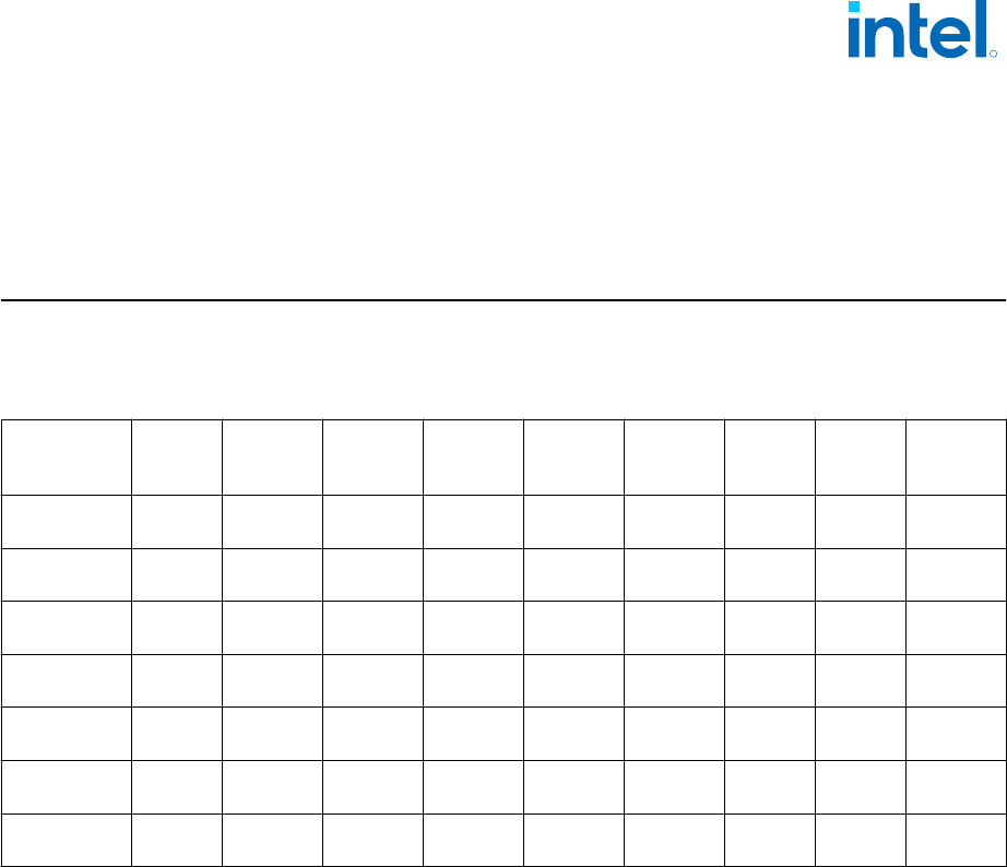
15.0 CPU And Device IDs
CPUID
Table 100. CPUID Format
SKU CPUID
Reserved
[31:28]
Extended
Family
[27:20]
Extended
Model
[19:16]
Reserved
[15:14]
Processo
r Type
[13:12]
Family
Code
[11:8]
Model
Number
[7:4]
Stepping
ID
[3:0]
S-processor
8+8
90672h Reserved 0000000b 1001b Reserved 00b 0110b 111b 0010b
HX SBGA -
processor 8+8
90672h Reserved 0000000b 1001b Reserved 00b 0110b 111b 0010b
S-processor
6+0
90675h Reserved 0000000b 1001b Reserved 00b 0110b 111b 0101b
P-processor
6+8
906A3h Reserved 0000000b 1001b Reserved 00b 0110b 1010b 0011b
H-processor
6+8
906A3h Reserved 0000000b 1001b Reserved 00b 0110b 1010b 0011b
U15-processor
2+8
906A4h Reserved 0000000b 1001b Reserved 00b 0110b 1010b 0100b
U9-processor
2+8
906A4h Reserved 0000000b 1001b Reserved 00b 0110b 1010b 0100b
• The Extended Family, Bits [27:20] are used in conjunction with the Family Code,
specified in Bits[11:8], to indicate whether the processor belongs to Intel
®
Core
™
processor family.
• The Extended Model, Bits [19:16] in conjunction with the Model Number, specified
in Bits [7:4], are used to identify the model of the processor within the processor's
family.
• The Family Code corresponds to Bits [11:8] of the EDX register after RESET, Bits
[11:8] of the EAX register after the CPUID instruction is executed with a 1 in the
EAX register, and the generation field of the Device ID register accessible through
Boundary Scan.
• The Model Number corresponds to Bits [7:4] of the EDX register after RESET, Bits
[7:4] of the EAX register after the CPUID instruction is executed with a 1 in the
EAX register, and the model field of the Device ID register accessible through
Boundary Scan.
• The Stepping ID in Bits [3:0] indicates the revision number of that model.
• When EAX is initialized to a value of '1', the CPUID instruction returns the
Extended Family, Extended Model, Processor Type, Family Code, Model Number
and Stepping ID value in the EAX register. Note that the EDX processor signature
value after reset is equivalent to the processor signature output value in the EAX
register.
15.1
R
CPU And Device IDs—12th Generation Intel
®
Core
™
Processors
12
th
Generation Intel
®
Core
™
Processors
February 2023 Datasheet, Volume 1 of 2
Doc. No.: 655258, Rev.: 010 205
Cache and TLB descriptor parameters are provided in the EAX, EBX, ECX and EDX
registers after the CPUID instruction is executed with a 2 in the EAX register.
PCI Configuration Header
Every PCI-compatible function has a standard PCI configuration header, as shown in
the table below. This includes mandatory registers (Bold) to determine which driver to
load for the device. Some of these registers define ID values for the PCI function,
which are described in this chapter.
Table 101. PCI Configuration Header
Byte3 Byte2 Byte1 Byte0 Address
Device ID Vendor ID (0x8086) 00h
Status Command 04h
Class Code Revision ID 08h
BIST Header Type Latency Timer Cache Line Size 0Ch
Base Address Register0 (BAR0) 10h
Base Address Register1 (BAR1) 14h
Base Address Register2 (BAR2) 18h
Base Address Register3 (BAR3) 1Ch
Base Address Register4 (BAR4) 20h
Base Address Register5 (BAR5) 24h
Card-bus CIS Pointer 28h
Subsystem ID Subsystem Vendor ID 2Ch
Expansion ROM Base Address 30h
Reserved
Capabilities
Pointer
34h
Reserved 38h
Maximum Latency Minimum Grant Interrupt Pin Interrupt Line 3Ch
Device IDs
This section specifies the device IDs of the processor.
Table 102. Host Device ID (DID0)
Platform Device ID
S LGA 8+8 4660h
S LGA 8+4 4668h
S LGA 6+4 4648h
S LGA 6+0 4650h
S LGA 4+0 4630h
S LGA 2+0 4610h
continued...
15.2
15.3
R
12th Generation Intel
®
Core
™
Processors—CPU And Device IDs
12
th
Generation Intel
®
Core
™
Processors
Datasheet, Volume 1 of 2 February 2023
206 Doc. No.: 655258, Rev.: 010
Platform Device ID
HX SBGA 8+8 4637h
HX SBGA 6+8 463Bh
HX SBGA 4+8 4623h
HX SBGA 4+8 462Bh
H 6+8 4641h
H 6+4 4649h
H 4+8 4621h
H 4+4 4629h
P 6+8 4641h
P 4+8 4621h
P 2+8 4601h
U15 2+8 4601h
U15 2+4 4609h
U15 1+4 4619h
U9 2+8 4602h
U9 2+4 460Ah
U9 1+4 461Ah
Table 103. Processor Graphics Device ID (DID2)
Platform
Processor
Step
GT SKU Device ID
S LGA 8+8 C0 32EU 4680h
S LGA 8+4 C0 32EU 4680h
S LGA 6+4 C0 32EU 4680h
S LGA 6+0 C0 24EU 4682h
HX SBGA 8+8 C0 32EU 4688h
HX SBGA 6+8 C0 32EU 4688h
HX SBGA 4+8 C0 32EU 4688h
HX SBGA 4+4 C0 16EU 468Bh
S LGA 6+0 H0 32EU 4690h
S LGA 6+0 H0 24EU 4692h
S LGA 6+0 H0 16EU 4693h
P 6+8 L0 96EU 46A6h
H 6+8 L0 96EU 46A6h
H 6+4 L0 64EU 46A3h
H 4+8 L0 80EU 46A6h
continued...
R
CPU And Device IDs—12th Generation Intel
®
Core
™
Processors
12
th
Generation Intel
®
Core
™
Processors
February 2023 Datasheet, Volume 1 of 2
Doc. No.: 655258, Rev.: 010 207

Platform
Processor
Step
GT SKU Device ID
H 4+4 L0 48EU 46A3h
P 6+8 L0 96EU 46A6h
P 4+8 L0 80EU 46A6h
P 2+8 L0 64EU 46B3h
U15 2+8 R0 96EU 46A8h
U15 2+8 R0 80EU 46A8h
U15 2+4 R0 64EU 46B3h
U15 1+4 R0 48EU 46B3h
U9 2+8 R0 96EU 46AAh
U9 2+8 R0 80EU 46AAh
U9 2+4 R0 64EU 46C3h
U9 1+4 R0 48EU 46C3h
Table 104. Other Device ID
Device Processor Line Bus / Device / Function DID
PCIe RC 010 G5 S, H, HX, P, U15 0 / 1 / 0 460Dh
PCIe RC 011 G5 S , HX 0 / 1 / 1 462Dh
Dynamic Tuning Technology
(DTT)
S, H, HX, P, U 0 / 4 / 0 461Dh
IPU(IMGU) H, P, U 0 / 5 / 0 465Dh
PCIe RC 060 (x4) G4 S, H, HX, P, U 0 / 6 / 0 464Dh
PCIe RC 062 (x4) G4 H, P, U15 0 / 6 / 2 463Dh
TBT PCIe0 H, P, U 0 / 7 / 0 466Eh
TBT PCIe1 H, P, U 0 / 7 / 1 463Fh
TBT PCIe2 H, P, U15 0 / 7 / 2 462Fh
TBT PCIe3 H, P, U15 0 / 7 / 3 461Fh
Gauss Newton Algorithm
(GNA)
S, H, HX, P, U 0 / 8 / 0 464Fh
Intel
®
Trace Hub S, H, HX, P, U 0 / 9 / 0 466Fh
Crash Log & Telemetry S, H, HX, P, U 0 / 10 / 0 467Dh
USB xHCI H, P, U 0 / 13/ 0 461Eh
USB xDCI H, P, U 0 / 13/ 1 460Eh
TBT DMA0 H, P, U 0 / 13/ 2 463Eh
TBT DMA1 H, P, U 0 / 13/ 3 466Dh
Intel
®
Volume Management
Device (VMD)
S,H, HX, P, U 0 / 14 / 0 467Fh
R
12th Generation Intel
®
Core
™
Processors—CPU And Device IDs
12
th
Generation Intel
®
Core
™
Processors
Datasheet, Volume 1 of 2 February 2023
208 Doc. No.: 655258, Rev.: 010
